|
|
  |
 |
|
|
|
|

Copyright © 2010
Created January 2, 2010
Updated January 27, 2010. See document history at end for details.
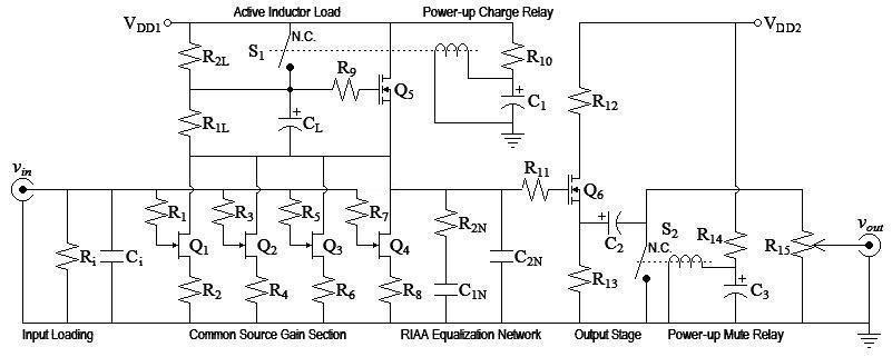
Active Inductor Example
Low-Noise JFET Phono Preamp
This is an example only. It is not intended to be final or complete design.This is a redesign using LSK170 JFETs on the input. You still may want to use the 2N3819 design because of the difficulty of obtaining LSK170's.
| Figure
1: Schematic |
||||||||||||||||||||||||||||||||||||||||||
 |
||||||||||||||||||||||||||||||||||||||||||
|
Initial Design Decisions
- Discrete voltage input design with 46db gain at 1kHz will amplify
5mV rms input to produce 1V rms
before attenuator.
- Q1-Q4 are LSK170 n-ch jfet (chosen for
excellent 1nV/rtHz noise specification). Use C grade to
accommadate current requirements.
- I chose four devices because multiple parallel devices devices increase S/N by sqrt(# of devices). In this case bettering the effective noise specification to 0.866nV/rtHz. (Gate and source resistor choices prevent ideal effective input noise of 0.5nV/rtHz)
- Q5,Q6 are BS170 n-ch mosfet (commonly available)
- vgs,max of Q6 of 20V limits VDD due to startup relays. Choose VDD = 18V.
- Let bias of active inductor set bias to gate of Q6 to eliminate coupling capacitor.
| vg,Q5 = | (VDD-vgs-Q5-max)+vsg-Q1-max
2 |
= |
18V-2V+8V
2 |
= 12V |
- R2L of active inductor functions as R1 of passive RIAA network.
- I chose to do the small signal class-a design with a fourier series based distortion predictor tool out of convenience. Small signal class-a design is not in the scope of this article.
- Because of possibility of negative feedback from buffer stage
back to gain stage through power supply, I decided to recommend two
power supply taps.
Gain Stage Design
Although I used a convenient fourier series analysis tool to do the small signal analysis, there were some design decisions. I wanted to choose gate and source resistors small enough to make their noise contribution insignificant compared to the JFET. This would lower noise and allow the possiblity of noise improvement with better JFETs.| Resistor
noise equation (per rtHz, figure of merit, does not account for
bandwidth) |
| vn-resistor-rtHz =
sqrt(4kTR) |
| R = |
vn-resistor-rtHz2
4kT |
= |
1nV2
4 x 1.3806504e-23 x 298.15ºK |
= 60.73254378Ω |
R1-R8 = 56Ω.
Because the fourier series analysis of this low noise design showed higher distortion than the 2N3819 version (but still very good) and because decreasing the source resistors furthur would increase the distortion, I made no furthur analysis with lower source resistor values.
Fourier Series Analysis of Q1-Q4 (excluding
drain load)
Analysis of Common Source Circuittransistor type = JFET
transconductance = 22mS
threshold voltage = -1V
source resistor = 56Ω
Input signal (peak) = 7.0710678mV
Input bias = 0V
Output signal (peak) = 72.364457µA
Output bias = 8.4337081mA
Gain = 10.23388mS
Total distortion = 22.089411nA = 0.03052522% = -70.3068dB
Breakdown by harmonic
| harmonic | value | percent | dB | |
| 0 | 8.4337302mA | 11654.52014075% | 41.33dB | DC Offset |
| 1 | 72.364457µA | 100.00000000% | 0.00dB | Fundamental |
| 2 | 22.089411nA | 0.03052522% | -70.31dB |
RIAA Analysis
Refer Calculating Passive RIAA Equalization in article Phono Equalization Calculations.From this fourier analysis we can calculate R1 of Passive RIAA network (aka R2L)
| R2L = |
(Low frequency RIAA boost
relative to 1kHz) x (1kHz output voltage)
(Output signal current) x (#parallel devices) |
= |
10 x 1.414213562V
72.364457µA x 4 |
= 48.85732655kΩ |
Given R1:R2 = 6.877358491
| R2N = | 48.7kΩ
6.877358491 |
= 7.081207133kΩ |
Given R1C1 = 2187µS
| C1N = |
2187µS
48.7kΩ |
= 44.90759754nF |
Choose parallel 5% value to makeup remainder: 2nF
C1N = 43nF + 2nF
Given R1C2 = 750µS
| C2N = |
750µS
48.7kΩ |
= 15.40041068nF |
Choose parallel 5% value to makeup remainder: 390pF
C2N = 15nF + 390pF
Active Inductor Analysis
Refer article Active Inductor Load.- Choose R2L for gain of overall circuit.
- Calculate/set gfs in preparation for remaining calculations, verifying bounds of equation (22). (equation (9))
gfs = 2 x sqrt(gmiD) = 2 x sqrt(320mS x 8.4337081mA x 4) = 207.7993876mS
- Choose R1L to set desired DC bias. (equation (24))
| R1L = |
R2L
|
= |
48.7kΩ
|
= 30.80342288kΩ |


- Choose CL to set the pole frequency the desired amount below the passband. (equation (21))
| CL = |
gfsR1L+1
2πfPOLER1L |
= |
(207.7993876mS x 30.9kΩ)+1
2π x 5Hz x 30.9kΩ |
= 6.615490071mF |
| fPOLE = |
gfsR1L+1
2πCLR1L |
= |
(207.7993876mS x 30.9kΩ)+1
2π x 10mF x 30.9kΩ |
= 3.307745035Hz |
- Determine if a bypass switch is needed to charge the capacitor on startup.
Calculate charge time for CL:
| i = C | δv δt |
| Δt = |
CΔv
iD |
= |
10mF x 2V
8.4337081mA x 4 |
= 592.8590296mSec |
Q6 Circuit Design
My design goal here was reasonably low output impedance. 1kΩ
output impedance would have been low enough to minimize voltage loss
into a typical 47kΩ load. I choose 500Ω instead on the far chance
of driving a 600Ω load with a tolerable voltage loss.Fourier Series Analysis of Q6 Circuit
Note: This analysis based on a more convenient equivalent model
of source circuit. Two 500Ω are modeled in series with one
bypassed by a capacitor in place of the parallel circuit shown.Analysis of Common Source Circuit
transistor type = MOSFET
transconductance = 320mS
threshold voltage = 2V
source resistor = 500Ω
Input signal (peak) = 1.4142136V
Input bias = 7V
Output signal (peak) = 2.7910912mA
Output bias = 9.8041739mA1
Gain = 1.9735995mS
Total distortion = 950.79116nA = 0.03406521% = -69.3538dB
Breakdown by harmonic
| harmonic | value | percent | dB | |
| 0 | 9.805058mA1 | 351.29836800% | 10.91dB | DC Offset |
| 1 | 2.7910912mA | 100.00000000% | 0.00dB | Fundamental |
| 2 | 888.84698nA | 0.03184586% | -69.94dB | |
| 3 | 56.727241nA | 0.00203244% | -93.84dB | |
| 4 | 4.7600566nA | 0.00017054% | -115.36dB | |
| 5 | 456.88194pA | 0.00001637% | -135.72dB |
Miscellaneous Calculations
R12 limits charge current through Q6 to C2 to <500mAR12 >= 20V/500mA = 40Ω
Choose R12 = 82Ω.
Want to set C2 for as low a highpass pole as CL. First find Requiv of pole. Output impedance of Q6 is the inverse of its operating ac transconductance gfs.
gfs = 2 x sqrt(gmiD) therefore
| Rout-Q6 = |
1
2 x sqrt(gmiD) |
= |
1
2 x sqrt(320mS x 9.8041739mA) |
= 8.92667066Ω |
| Requiv = (Rout-Q6 || R13) + R15 = | Rout-Q6 x R13
Rout-Q6 + R13 |
+ R15 = 1.00884769kΩ |
| C2 = |
1
2πfpoleRequiv |
= |
1
2π x 3.307745035Hz x 1.00884769kΩ |
= 47.69386318µF |
Choose R10 and R14 to set 10mA through relay coil.
| R10 = |
VDD-vCOIL
iCOIL |
= |
18V-5V
10mA |
= 1.3kΩ |
Calculate load current from power supplies VDD1 and VDD2.
iDD1 = iQ1-BIAS x 4 + iRELAYCOIL = 8.4337081mA x 4 + 10mA = 43.7348324mA
iDD2 = iQ6-BIAS + iRELAYCOIL = 9.8041739mA + 10mA = 19.8041739mA
Design Decisions Left to You
- Ri and Ci should be calculated per article Phono Termination Calculations and Calculator.
- Gate resistors were somewhat arbitrarily chosen. They seem
to be good values. I know that the 1kΩ values work with the
BS170. I have seen many jfet schematics without gate resistors at
all. Increase them if any oscillations occur. Because the
gate resistor noise in this design is the same as that of the JFET
chosen, I suggest trying to lower or eliminate gate resistors on the
JFETs, so long as they do not oscillate.
- Relay components C1 and C3 must be calculated as follows:
- This circuit and its analysis is only given as an example; change everything if you like.
- A low noise 18V power supply. I recommend the circuit of
article Line Level Class A Power Supply.
|
|
1There is a seeming discrepancy
in the fourier
analysis between the cited output bias and the same value given in the
analysis. The first value is the bias without any signal and the
second with a signal. This effect is created by the same asymetrical
transfer curve that gives us a desireable second order distortion
characteristic. The positive half of the signal is amplified more
than the negative half. As a result the dc bias is modulated by
the average signal level. This small component amounts to AM
demodulation of the music signal. Abstractly, I had already
anticipated this effect. I would be curious what effect this has
on the overall sound. Is is detrimental, or does it add an extra
euphonic bass urge?
Document History
January 2, 2010 Created
January 2, 2010 Minor Updates.
January 5, 2010 Recommend split power supply to prevent
feedback.
Update schematic to show change. Recommend specific power supply.
January 5, 2010 Choose relays S1 and S2, calculate their series
resistors, and calculate specific load current for each power supply
tap.
January 9, 2010 Added footnote explaining how fourier series
analysis
shows modulation of dc bias by music signal.
January 17, 2010 Added design criteria for class-a biasing
decisions.
January 17, 2010 Create new version of document based on LSK170
input JFETs. Only Gain stage, RIAA, and Active Inductor analyses
changed.
January 22, 2010 Minor Corrections. Modify schematic for
clarity. Capacitor cited wrong in CL charge time
calculation. Calculated result already correct.
Change C2 calculation to match CL pole.
Kept same C2 choice.
January 23, 2010 Correct schematic in vicinity of Q4, R7,
and R2N.
January 27, 2010 Minor improvement to writing
style.