Copyright © 2009 by Wayne Stegall
Updated March 11, 2010. See
Document History at end for
details.
Active Inductor Load
Introduction
Attempts to get high gain from one class A amplication stage
are complicated by the fact that that output DC bias increases with
this same gain. The result is either limited gain or some
absurdly large collector/drain power supply. The obvious solution
would be to load the output with an impedance that is sufficiently high
in the passband to give the desired gain but low enough at DC to allow
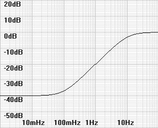
reasonable bias voltages. A sample response is given in
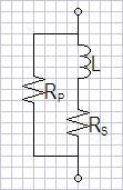
figure 1 and the passive circuit model in figure 2. In the model
of figure 2, RP represents the desired passband load, RS
sets the DC bias, and L sets the pole (and the zero) to fall below the
passband.
Figure
1: Bode plot of typical impedance
|
Figure
2: Passive model
|
|
|
It happens that this is the passive equivalent of the simplest of
active inductors. This is fortunate because the passive circuit
would require an impossibly large inductor in this application.
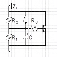
Figure 3 shows this active inductor and figure
4 shows its simplified ac model. If you have another application
for an active inductor, remember that the circuit only models an
inductor in the sloped region between the zero and the pole.
Figure
3: Active Inductor
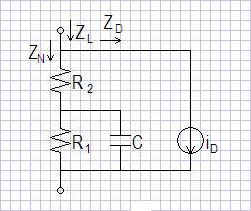
|
Figure
4: AC model
|
|
|
|
iD = gfsvC
|
Design Summary
- Choose R2 for gain of overall circuit.
- Calculate/set gfs in preparation for remaining
calculations, verifying bounds of equation (22).
(equation (9))
- Choose R1 to set desired DC bias. (equation (24))
- Choose C to set the pole frequency the desired amount below the
passband. (equation (21))
- Determine if a bypass switch is needed to charge the capacitor on
startup.
Passive Circuit Analysis
As a point of comparison, analyze passive circuit of
figure
2.
(1)
|
Z(s) = RP || ( sL+RS)
|
(2)
|
|
RP(sL+RS) |
|
sLRP+RPRS |
|
Z(s) =
|

|
=
|
|
|
|
RP+sL+RS |
|
sL+RP+RS |
(3)
|
|
RPRS |
|
RS |
|
RS |
|
ωZERO
=
|
|
=
|
|
, fZERO
=
|
|
|
|
LRP |
|
L |
|
2πL
|
(4)
|
|
RP+RS |
|
RP+RS |
|
ωPOLE
=
|
|
, fPOLE
=
|
|
|
|
L |
|
2πL
|
Determination of AC Forward Transconductance
It is necessary to calculate the ac transconductance to continue with
the calculations. Many
symbols are used for transconductance such as G
m, g
fs,
and
g
m. I have decided choose and g
fs for
the ac
transconductance, and k
n for the transconductance figure of
merit in
the MOSFET model below.
(5)
|
MOSFET model1
|
|
(6)
|
Simplified model
|
(7)
|
The same solved for v
|
|
iD = kn(vgs
- vT)2
|
, to simplify calculations let v
= vgs
- vT,
|
|
iD = knv2 |
|
v = sqrt(iD/kn)
|
Derive g
fs by differentiating the simplifed MOSFET model
with respect to v.
(8)
|
|
δiD |
|
|
|
(9)
|
|
|
|
|
|
|
gfs =
|
|
= 2knv
|
, substitute v from
equation (7):
|
gfs = 2knsqrt(iD/kn),
|
|
gfs = 2 x sqrt(kniD) |
|
|
|
|
|
|
δv |
|
|
|
|
|
|
|
|
|
If you do not have a specification for k
n from which to
calculate g
fs, you will have to determine it some other
way. Perhaps inspection of a graph. If you are given g
fs,
you
can
rearrange
equation (9) to solve for k
n.
Furthermore, you may alter the effective g
fs for any reason
(i.e. g
fs parameter stability) by adding a source resistor:
(10)
|
|
gfs |
|
gfs-effective =
|
|
|
|
gfsRsource+1
|
Active Circuit Analysis
It would be easy to presume that the analysis of
figure
4 would just be determined
from R
1, R
2, and C. However this circuit
has current feedback
from the drain back to the biasing network, and must be analyzed more
thoroughly.
|
|
,
|
(14)
|
|
vin
|
|
sR1R2C+(R1+R2)
|
|
ZD =
|
|
=
|
|
|
|
iD
|
|
gfsR1
|
|
|
(15)
|
|
R1
|
|
(16)
|
|
sR1R2C+(R1+R2)
|
|
ZN = R2+R1||C
=
R2+
|
|
,
|
|
ZN =
|
|
|
|
sR1C+1
|
|
|
|
sR1C+1
|
(17)
|
|
1
|
|
1
|
|
1
|
|
|
(sR1C+1)+gfsR1 |
|
YL =
|
|
=
|
|
+
|
|
,
|
YL =
|
|
|
|
ZL
|
|
ZN
|
|
ZD
|
|
|
sR1R2C+(R1+R2) |
(18)
|
|
sR1R2C+(R1+R2) |
|
ZL =
|
|
|
|
sR1C+(gfsR1+1) |
A zero and a pole!
(19)
|
|
R1+R2 |
|
R1+R2 |
|
ωZERO
= |
|
, fZERO
= |
|
|
|
R1R2C |
|
2πR1R2C |
(20)
|
|
gfsR1+1 |
|
gfsR1+1 |
|
ωPOLE
=
|
|
, fPOLE
=
|
|
|
|
R1C |
|
2πR1C |
Practical Boundaries to Component Selection
For our application, we want to choose C so that the pole does not
affect the passband. Derive from equation (20):
(21)
|
|
gfsR1+1 |
|
C =
|
|
|
|
2πfPOLER1 |
We want ω
POLE >> ω
ZERO.
| gfsR1+1 |
|
R1+R2 |
|
gfsR1R2+R2 |
|
R1+R2 |
|
|
>>
|
|
,
|
|
>>
|
|
,
|
| R1C |
|
R1R2C |
|
R1R2C |
|
R1R2C |
|
| gfsR1R2+R2
>> R1+R2 , gfsR1R2
>> R1 |
Any reasonable choice of R
2 would likely meet this condition.
DC Analysis
Our application sets R
2 for desired circuit gain. Now
calculate
R
1 for desired DC bias (v
bias). The
gate-source voltage (v
gs)
driven by
the bias current is multiplied by the R
1-R
2
resistor divider. The first equation is the product of the
resistor divider factor and the MOSFET equation (5) solved for v
gs.
Note
that
i
D here is the DC drain current.
|
R1vbias |
|
| R1+R2
= |
|
, R2
= R1 |
|
vT+sqrt(iD/kn) |
|
|
 |
| vbias |
|
|
-1
|
| vT+sqrt(iD/kn) |
|
|
 |
(24)
|
|
R2 |
|
R1 = |
|
|
|
|
If you used a source resistor to modify g
fs add the source
resistor
voltage to v
T in these equations:
(25)
|
vT-effective = vT
+ iDRsource
|
If v
T >> sqrt(i
D/k
n)
(a fairly common assumption),
an approximate DC analysis is acceptable instead of equation (24).
(26)
|
|
R2 |
|
R1 = |
|
|
|
|
Example to come...
1Donald L. Schilling, Charles
Belove, Electronic Circuits: Discrete and Integrated (New York,
1979), p. 143 equation (3.2-2b)
Document History
October 21, 2009 Created.
October 23, 2009 corrected equation (21).
March 3, 2010 Added equation (26) for approximate DC
analysis.
March 11, 2010 Changed designation for MOSFET constant to proper kn.