 |
| Home │ Audio
Home Page |
Copyright © 2010 by Wayne Stegall
Updated March 26, 2011. See document history at end for
details.
Low-Noise Two-Stage JFET Phono Preamp
This circuit is SPICE verified. It is only provided for design assistance. Its final validity awaits someone to prototype it.
| Figure
1:
Schematic |
||||||||||||||||||||||||||||||||||||||||||||
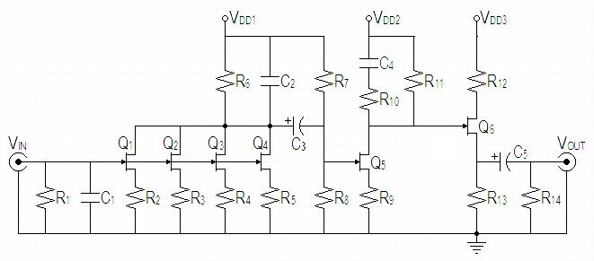 |
||||||||||||||||||||||||||||||||||||||||||||
** Capacitor pairs are connected in parallel. Verify parts list to final SPICE model. |
Initial Design Decisions
- Design approach is to use higher voltage power supply to allow larger gain with conventional class A circuits.
- Want 5mVRMS to produce 1VRMS at output at 1kHz. This amounts to 46dB of gain at 1kHz. Most gain references and calculations are relative to 66dB of gain below 50Hz. Altered gain goal to standard RIAA 40dB of gain at 1kHz to lower distortion.
- Initially choose 48V power supplies because of unsatisfactory results with 40V supply in prior design cycle.
- Q1-Q5 are LSK170A n-ch jfet (chosen for excellent 1nV/√Hz noise specification). Use A grade for more possible gain.
- Desireable self bias (Vg-dc = 0V, all bias set by source resistor) on first stage is allowed by small input signal. (Signal will clip if peak is greater than Vp0 of -0.4025156V; distortion considerations require even more headroom.)
- That a larger signal drives second stage requires more bias than self bias would allow. Use gate biasing for second stage.
- I chose four devices for stage one because multiple parallel devices devices increase S/N by sqrt(# of devices). In this case halving the effective noise in the source circuit and to some extent overall.
- Q6 is LSK170C n-ch jfet. Biasing concerns disadvantage MOSFET here.
- Because of possibility of negative feedback from buffer stage back to gain stage through power supply, I decided to recommend three power supply taps.
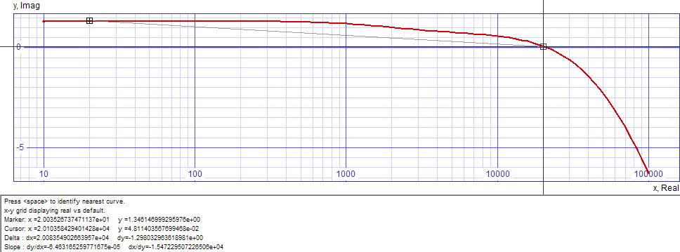
| Figure
2:
Stage
with
75µS
pole
(red
curve)
will
boost
signal out of
noise quicker in first stage than one with 3180µS
pole
and
318µS zero (black curve). |
 |
Gain Stage Design
As an Initial observation, a higher gate bias in the second stage forced by the gain of the first stage would cause the first stage to bear a greater share of the overall gain.| Figure 3: LSK170A SPICE model for reference |
| .MODEL LSK170A NJF + BETA = 0.0378643 VTO = -0.4025156 LAMBDA = 4.783719E-3 + IS = 3.55773E-14 + RD = 10.6565 RS = 6.8790487 + CGD = 3.99E-11 CGS = 4.06518E-11 + PB = 0.981382 FC = 0.5 + KF = 0 AF = 1 |
Stage One
I wanted to choose source resistors small enough to make their noise contribution insignificant compared to the JFET. This would lower noise and allow the possiblity of noise improvement with better JFETs.| Resistor
noise
equation
(per
√Hz, figure of merit,
does not account for
bandwidth) |
| vn-resistor-rtHz =
sqrt(4kTR) |
| R = |
vn-resistor-rtHz2
4kT |
= |
1nV2
4 x 1.3806504e-23 x 298.15ºK |
= 60.73254378Ω |
R2-R5 = 56Ω.
Some initial conditions would allow direct computation of bias, but iteration (repetitive computer calculations) or a load line graph are required to calculate the current bias to begin small signal analysis from the parameters given (Vgs-dc = 0V and Rs = 56Ω).
Given kn (BETA) = 37.8643mA/V2 and VT = -402.5156mV for LSK170A, bias current iterates to 2.551918mA.
Given LAMBDA = 4.783719m(V-1) from LSK170A spice model calculate rds:
| rds = |
1
LAMBDA x iD0 |
= |
1
4.783719m(V-1) x 2.551918mA |
= 81.9159kΩ |
| ID = 2.551918mA + |
4V
81.9159kΩ |
= |
2.60075mA |
Calculate gfs and make a rough estimate of maximum possible gain to continue calculations. (This is a situation where we need to know the gain before we actually calculate it.)
gfs = 2 x sqrt(knID) = 2 x sqrt(37.8643mA/V2 x 2.60075mA) = 19.8470mS
| AV-preliminary = |
Apparent max load bias voltage
|VGS| |
= |
VDD - 2|VT-max|
ID x (Rs + 1/gfs) |
= |
48V - 2(2V)
2.60075mA x (56Ω + 1/19.8470mS) |
= 159.0273565(V/V) |
Want drain load much less than rds/4 to minimize affect of parameter variance on equalization. Calculate bias limit on Rd:
| Rd <= |
VDD - (VG+|VT-max|)
-
(vg-peak x AV-preliminary) - (VDRAIN-SAFETY-FACTOR)
ID x 4 |
= |
48V - (0V + 2V) - (14mV x
159.0273565) - 4V
2.60075mA x 4 |
= 3.82328kΩ |
We must know Input bias to second stage to finish calculations for first stage.
Make a more refined gain estimate for stage 1 to set stage 2 input bias:
| AV-refined = |
4 x Rd-total Rs + 1/gfs |
= |
4 x (R6 || (rds/4)) Rs + 1/gfs |
= |
4 x (3.74kΩ || 20.479kΩ)
56Ω + 1/19.8470mS |
= 118.906(V/V) |
vg-peak-stage2 = vg-peak-stage1 x 14mV = 118.906 x 14mVpeak = 1.66468Vpeak
| AV-stage2 = |
AV-total
AV-stage1 |
= |
2000
118.906 |
= 16.82(V/V) |
| Vbias-stage2 = |
VDD - |VT-max|
-
vg-peak-stage2 - (VDRAIN-SAFETY-FACTOR)
(AV-stage2 + 1) + AV-SAFETY-FACTOR |
= |
48V - 2V
- 1.66468V - 4V
20 |
= 2.01677V |
Choose R7 = 10MΩ, calculate R8:
| R8 = 10MΩ x |
Vbias-stage2
VDD - Vbias-stage2 |
= 10MΩ x |
2V
48V - 2V |
= 434.783kΩ |
Calculate actual bias with standard values:
| Vbias-stage2 = |
48V x 442kΩ
10MΩ + 442kΩ |
= 2.03179V |
Calculate final gain.
| AV-stage1 = |
4 x Rd-total Rs + 1/gfs |
= |
4 x (R6 || R7
|| R8 || (rds/4)) Rs + 1/gfs |
= |
4 x (3.74kΩ || 10MΩ || 442kΩ ||
20.479kΩ)
56Ω + 1/19.8470mS |
= 118.024 = 41.4394dB |
After stage 2 gain established, I decide to recalculate R6 for standard RIAA gain to get less distortion. (Here -|| means subtract from parallel combination)
| AV-stage1-new = |
1000
AV-stage2 |
= |
1000
13.3985 |
= 74.6352(V/V) |
| R6 = | AV-stage1(Rs
+ 1/gfs)
4 |
-|| (R7 || R8 || (rds/4)) = | 74.6352(56Ω +
1/19.8470mS)
4 |
-|| (10MΩ || 442kΩ || 20.479kΩ) = | 1.98502kΩ -|| 19.5339kΩ |
| R6 = |
19.5339kΩ x 1.98502kΩ
19.5339kΩ - 1.98502kΩ |
= 2.20955kΩ |
Stage Two
Calculate rds: from LAMBDA and desired 2mA bias| rds = |
1
LAMBDA x iD0 |
= |
1
4.783719m(V-1) x 2mA |
= 104.521kΩ |
| ID = 2mA + |
4V
104.521kΩ |
= |
2.03827mA |
VG = RsID + VT + sqrt(ID/kn)
RsID = VG - VT - sqrt(ID/kn)
| Rs = |
VG - VT
- sqrt(ID/kn)
ID |
= |
2.03179V - -402.5156mV -
sqrt(2.03827mA/37.8643mA/V2)
2.03827mA |
= 1.08047kΩ |
This little round to standard value does not merit recalculation of ID.
Calculate bias limit on Rd:
| Rd <= |
VDD - VG -
|VT-max|
-
vd-peak - (VDRAIN-SAFETY-FACTOR)
ID |
= |
48V - 2.03179V - 2V - 2.82843V -
4V
2.03827mA |
= 18.2212kΩ |
gfs = 2 x sqrt(knID) = 2 x sqrt(37.8643mA/V2 x 2.03827mA) = 17.5702mS
Calculate Rd for desired total gain of 66dB
| AV-stage2-target = 16.82(V/V) = | Rd-total Rs + 1/gfs |
= |
R11 || rds Rs + 1/gfs |
Subtract rds from parallel Rd-total combination:
| R11 = |
rds x Rd-total
rds - Rd-total |
= |
104.521kΩ x 19.4593kΩ
104.521kΩ - 19.4593kΩ |
= 23.911kΩ |
Choose next lower 1% standard value: R11 = 18.2kΩ
Calculate gain shortfall:
| AV-stage2-actual
= |
Rd-total Rs + 1/gfs |
= |
R11 || rds Rs + 1/gfs |
= |
18.2kΩ || 104.521kΩ
(1.1kΩ + 1/17.5702mS) |
= 13.3985(V/V) |
AV-LOSS = 13.3985/16.82 = 796.582m
AV-LOSS-dB = 20log10(796.582m) = -1.97539dB
This is an acceptable design compromise.
SPICE shows distortion more than I would like.
Went back and recalculated R6 of stage 1 for overall RIAA standard 40dB of gain at 1kHz to lower distortion.
Calculate input capacitance to prepare to evaluate its affect on RIAA network of previous stage (These formulas are those to calculate reverse-bias diode capacitance which the gate forms with respect to both the drain and the source.):
| CGS = |
CGS
(1 - VGS/PB)0.5 |
= |
CGS
(1 - (VT + sqrt(ID/kn))/PB)0.5 |
| CGS = |
4.06518e-11
(1 - (-402.5156mV + sqrt(2.03827mA/37.8643mA/V2))/0.981382)0.5 |
= 37.5228pF |
| CGD = |
CGD
(1 - VGD/PB)0.5 |
= |
CGD
(1 - (VG - VDD)/PB)0.5 |
| CGD = |
3.99e-11
(1 - (2.03179V-(48V - 2.03827mA x 18.2kΩ))/0.981382)0.5 |
= 12.5923pF |
| CG = CGS + CM = CGS + CGD(AV + 1) = 37.5228pF + 12.5923pF(1.33985 + 1) = 66.9869pF |
Output Buffer
| Figure 4: LSK170C SPICE model for reference. |
| .MODEL LSK170C
NJF + BETA = 0.0278541 VTO = -0.800434 LAMBDA = 0.0122435 + IS = 2.45217E-14 + RD = 12 RS = 5.8 CGD = 4.22E-11 + CGS = 4.23E-11 PB = 0.9265487 + FC = 0.5 KF = 0 AF = 1 |
R12 limits short-circuit current through Q6 to 20mA
R12 >= 48V/20mA = 2.4kΩ.
Choose 5% value: R12 = 2.4kΩ.
Calculate VG .
VG = VDD - iD-Q5R11 = 48V - 2.03827mA x 18.2kΩ = 10.9035V
Min iDSS of 10mA sets ID limit. Choose half at ID = 5mA.
Calculate rds: from LAMBDA and desired 5mA bias
| rds = |
1
LAMBDA x iD0 |
= |
1
0.0122435(V-1) x 5mA |
= 16.3352kΩ |
| Rs = |
VG - VT
- sqrt(ID/kn)
ID |
= |
10.9035V - -800.434mV -
sqrt(5mA/0.0122435A/V2)
5mA |
= 2.21298kΩ |
Output impedance of Q6 is the inverse of its operating ac transconductance gfs.
gfs = 2 x sqrt(knID) therefore
| Rout-Q6 = |
1
2 x sqrt(knID) |
= |
1
2 x sqrt(27.8541mA/V2 x 5mA) |
= 42.3682Ω |
Arbitrarily choose 5% value, R14 = 100kΩ, only to ground output capacitor C5.
Calculate input capacitance to prepare to evaluate its affect on RIAA network of previous stage:
| CGS = |
CGS
(1 - VGS/PB)0.5 |
= |
CGS
(1 - (VT + sqrt(ID/kn))/PB)0.5 |
| CGS = |
4.23e-11
(1 - (-800.434mV + sqrt(5mA/27.8541mA/V2))/0.9265487)0.5 |
= 35.6658pF |
| CGD = |
CGD
(1 - VGD/PB)0.5 |
= |
CGD
(1 - (VG - VD)/PB)0.5 |
| CGD = |
4.22e-11
(1 - (10.9035V - (48V - (5mA x 2.4kΩ)))/0.9265487)0.5 |
= 7.96283pF |
| AV-buffer = |
Rd-total Rs + 1/gfs |
= |
R12 || rds Rs + Rout-Q6 |
= |
2.4kΩ || 16.3352kΩ
2.4kΩ + 42.3682Ω |
= 856.774m(V/V) |
| CG = CGS + CM = CGS + CGD(AV + 1) = 35.6658pF + 7.96283pF(856.773m + 1) = 50.451pF |
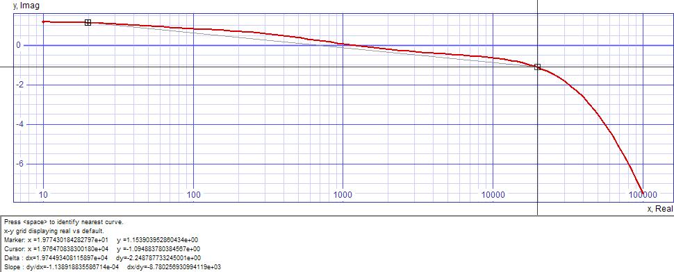
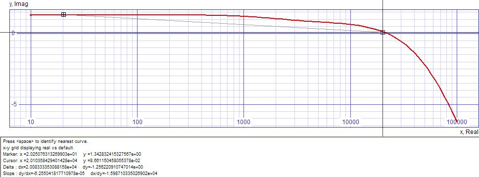
RIAA Analysis
Stage OneCalculate the effective network resistance and solve C2 for a pole of 75µS.
R6-network = R6 || R7 || R8 || (rds/4) = 2kΩ || 10MΩ || 442kΩ || 20.479kΩ = 1.81425kΩ
| C2-network = |
Tpole
R6-network |
= |
75µS
1.81425kΩ |
= 41.3395nF |
| C2 = C2-network - CG-stage2 = 41.3395nF - 66.9869pF = 41.2725nF |
Stage Two
Calculate the effective DC network resistance and solve for
R11-network = R11 || rds = 18.2kΩ || 104.521kΩ = 15.5009kΩ
R10 = R11 / 9 = 15.5009kΩ / 9 = 1.72232kΩ
| C4 = |
Tzero
R10 |
= |
318µS
1.72232kΩ |
= 184.635nF |
Adjustments
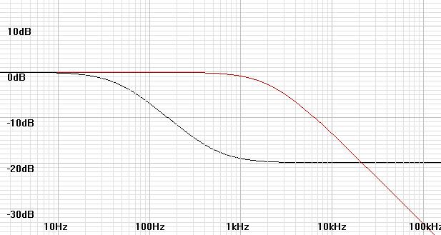
In spite of careful calculations, the RIAA network values will require adjustments during SPICE evaluation due to unexpected and stray effects. Even then, rounding to standard values will require experimentation to get best frequency response curve. The parts list will show these changes.SPICE evaluation of unadjusted design circuit was immediately excellent. The somewhat wavy gain plot sloped down from 20Hz to 20kHz by only 2.25dB.
| Figure
5:
Frequency
response
of
unadjusted
design
circuit |
 |
| SPICE Model, LSK170 SPICE Subckt Models |
Optimizing RIAA network values in SPICE rids plot of waviness to slope down from 20Hz to 20kHz by only 1.60dB. Calculations for adjustments are made in the following linear manner. If measurement increases with increase in component value, calculate adjustment by:
| valuenew = | valuecurrent x |
measurementtarget
measurementobserved |
| valuenew = | valuecurrent x |
measurementobserved
measurementtarget |
| Figure 5: Frequency response of SPICE optimized circuit |
 |
| SPICE Model, LSK170 SPICE Subckt Models |
After careful rounding of component values plot slopes down from 20Hz to 20kHz by only 1.30dB.
| Figure
6:
Frequency
response
of
final
circuit
after
choosing
standard
component
values. |
 |
| SPICE Model, LSK170 SPICE Subckt Models |
Higher than anticipated JFET transconductance may require raising supply voltage to prevent drain saturation. Unexpected distortion of prototype may be aleviated by raising power supply voltage.
Other SPICE Findings
SNR = 102.98dB relative to 1Vrms output. This would be relative to a 10mV cartridge output amplified by 40dB gain at 1kHz. SNR will vary with cartridge output after you compensate with your volume control.Fourier analysis for vout: (Distortion performance at 7.071mVpeak(5mVrms) and 1kHz and breakdown by harmonic)
Fourier analysis for vout:
No. Harmonics: 10, THD: 0.0178052 %, Gridsize: 200, Interpolation Degree: 1
| Harmonic | Frequency | Magnitude | Phase | Norm. Mag | Norm. Phase |
| -------- | --------- | --------- | ----- | --------- | ----------- |
| 0 | 0 | 0 | 0 | 0 | 0 |
| 1 | 1000 | 0.879288 | -92.635 | 1 | 0 |
| 2 | 2000 | 0.000146834 | -19.801 | 0.000166992 | 72.8345 |
| 3 | 3000 | 5.41796e-005 | -38.326 | 6.16175e-005 | 54.3094 |
| 4 | 4000 | 3.23322e-006 | -95.464 | 3.67709e-006 | -2.8289 |
| 5 | 5000 | 1.56558e-006 | -131.85 | 1.78051e-006 | -39.21 |
| 6 | 6000 | 3.12765e-007 | -88.13 | 3.55703e-007 | 4.50502 |
| 7 | 7000 | 1.21373e-006 | -45.309 | 1.38036e-006 | 47.3267 |
| 8 | 8000 | 2.42554e-007 | -80.335 | 2.75853e-007 | 12.3003 |
| 9 | 9000 | 7.75152e-007 | 58.3996 | 8.81568e-007 | 151.035 |
Fourier analysis for vout: (Distortion performance at 100Hz and proportionate level to 1kHz and breakdown by harmonic)
No. Harmonics: 10, THD: 0.0190292 %, Gridsize: 200, Interpolation Degree: 1
| Harmonic | Frequency | Magnitude | Phase | Norm. Mag | Norm. Phase |
| -------- | --------- | --------- | ----- | --------- | ----------- |
| 0 | 0 | 0 | 0 | 0 | 0 |
| 1 | 100 | 0.891848 | -90.243 | 1 | 0 |
| 2 | 200 | 0.000169612 | 170.701 | 0.00019018 | 260.944 |
| 3 | 300 | 5.79251e-006 | -75.974 | 6.49495e-006 | 14.2693 |
| 4 | 400 | 3.3312e-007 | 49.7897 | 3.73516e-007 | 140.033 |
| 5 | 500 | 2.1084e-007 | 94.8152 | 2.36408e-007 | 185.058 |
| 6 | 600 | 1.69153e-007 | 96.0689 | 1.89666e-007 | 186.312 |
| 7 | 700 | 1.44333e-007 | 96.9693 | 1.61835e-007 | 187.212 |
| 8 | 800 | 1.2705e-007 | 97.6061 | 1.42457e-007 | 187.849 |
| 9 | 900 | 1.13432e-007 | 98.8471 | 1.27188e-007 | 189.09 |
Fourier analysis for vout: (Distortion performance at 10kHz and proportionate level to 1kHz and breakdown by harmonic)
No. Harmonics: 10, THD: 0.345553 %, Gridsize: 200, Interpolation Degree: 1
| Harmonic | Frequency | Magnitude | Phase | Norm.Mag | Norm.Phase |
| -------- | --------- | --------- | ----- | --------- | ----------- |
| 0 | 0 | 0 | 0 | 0 | 0 |
| 1 | 10000 | 0.821345 | -102.31 | 1 | 0 |
| 2 | 20000 | 0.00283777 | -107.17 | 0.00345502 | -4.8656 |
| 3 | 30000 | 4.86413e-005 | -79.038 | 5.92215e-005 | 23.2697 |
| 4 | 40000 | 2.79079e-006 | 168.487 | 3.39783e-006 | 270.794 |
| 5 | 50000 | 9.02139e-007 | -74.142 | 1.09837e-006 | 28.1659 |
| 6 | 60000 | 9.62636e-007 | -84.247 | 1.17202e-006 | 18.0606 |
| 7 | 70000 | 8.13981e-007 | -83.821 | 9.91034e-007 | 18.4866 |
| 8 | 80000 | 7.11331e-007 | -82.815 | 8.66056e-007 | 19.4925 |
| 9 | 90000 | 6.33031e-007 | -81.892 | 7.70725e-007 | 20.4162 |
Miscellaneous Calculations
Now set coupling capacitor values C3 and C5 for best bass response:Initially desire both highpass poles at 0.1Hz for nearly no affect at 20Hz.
Rpole = R6 || (rds/4) + R7 || R8 = 2kΩ || 20.479kΩ + 10MΩ || 442kΩ = 1.82206kΩ + 423.291kΩ = 425.113kΩ
| C3 = |
1
2πfpoleRpole |
= |
1
2π x 0.1Hz x 425.113kΩ |
= 3.74383µF |
Assuming a high impedance load (RL >= 10kΩ):
Rpole = Rout-Q6 + R14 || RL = 42.3682Ω + 100kΩ || 10kΩ = 9.13328kΩ
| C5 = |
1
2πfpoleRpole |
= |
1
2π x 0.1Hz x 9.13328kΩ |
= 174.258µF |
If you want a polyethylene capacitor here choose C5 = 10µF and recalculate pole:
| fpole = |
1
2πC5Rpole |
= |
1
2π x 10µF x 9.13328kΩ |
= 1.74258Hz |
You may recalculate C5 if you want to drive 600Ω.
Calculate load current from power supplies VDD1, VDD2, and VDD3.
iDD1 = iQ1-BIAS x 4 + iR7-R8 = 2.551918mA x 4 + 48V/(10MΩ + 442kΩ) = 10.2123mA
iDD2 = iQ6-BIAS = 2.03827mA
iDD3 = iQ6-BIAS = 5mA
Design Decisions Left to You
- R1 and C1 should be calculated per article Phono Termination Calculations and Calculator.
- This circuit and its analysis is only given as a design example; change everything if you like.
- A low noise 48V power supply. The Line Level Class A Power Supply presented earlier will require a design improvement to deliver 48V. The LM317 used as a preregulator has a 40V limit on the input/output differential. See the LM317 datasheet for ideas.
- Whether protection zeners (39V) should be used to protect from drain overvoltage. (Connected from drain to source or ground.) Load resistors may provide sufficient protection.
- Resistor wattage given for normal operation. Decide whether
more wattage is needed at power up.
- In spite of careful design, transistor parameter variations may
require more adjustments during the prototyping process. The
specifications in this design are only valid if the JFETs match the
SPICE model parameters. ;=(
|
|
Document History
June 26, 2010 Created
July 3, 2010 Recalculated with 48V power supply and RIAA standard
gain.
January 26, 2011 Removed personal comment at
beginning. Made minor symbol improvements.
March 26, 2011 Corrected numerical typo at end of first stage
calculations not affecting their results and a misspelling in the SPICE
results.