 |
| Home │ Audio
Home Page |
Copyright © 2012 by Wayne Stegall
Updated July 8, 2012. See Document History at end for
details.
Floating Source-follower Regulator
One-Bend Amplifier
Part 4: Hum injected in stage 2 of amplifier required the design
of a useful
general purpose voltage regulator.
Introduction
At the moment that I realized that the inner feedback loop added to the amplifier for its desirable attributes connected ripple from the VDD1 supply line into open-loop signal path, it became necessary to regulate the offending voltage. I already held this regulator in my mind as one for non-feedback circuits to get the maximum voltage out that the properties of the regulating MOSFET would allow.Regulator Design
The operation of the regulator in figure
1 below is based on a MOSFET
being in current amplification mode if the following condition is met.| (1) |
VDS > VGS - VT. |
With VDS ≈ VGS, regulation is possible if negative ripple deviation does not exceed ≈2VT.
R1 and C1 filter ripple to a level low enough to be eliminated by the diode filter comprised of the parallel diodes and C3. VG then takes the average of the ripple peaks and dips in VD. Assuming VG is filtered to a constant value:
| (2) |
VDS = VGS ± ½vpeak-ripple |
Take the ripple dip as worst case
| (3) |
VDS = VGS - ½vpeak-ripple |
Combine equations 1 and 3 to get:
| (4) |
VGS - VT < VGS - ½vpeak-ripple |
Solve to get design equation
| (5) |
vpeak-ripple < 2VT. |
| Figure
1:
Floating
source-follower
regulator |
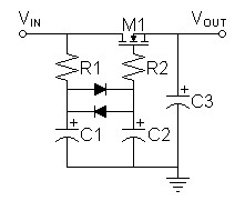 |
Design Methodology
- Calculate capacitance in preceding raw supply to give ripple less than 2VT of regulating MOSFET.
- Calculate R1 for balance between low noise and reasonable current limits.
- Calculate C1 for a RC constant giving ripple low enough at input
to
diode filter to allow diode impedance high enough to eliminate the
remaining ripple. Initially 25mV seems a good target because it
is a figure of merit in the real diode equation.
- Arbitrarily choose C2 to give high RC constant appropriate for expected high Z of parallel diodes, then adjust if necessary during simulation.
- Choose R2 as normal to prevent LC oscillations in regulating MOSFET.
- Calculate C3 to give desired suppression of nonlinearity of regulating MOSFET.
| Figure
2:
Floating
source-follower
regulator
clamped
to
ripple
minimum |
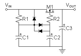 |
The only change in design methodology is the added difficulty in calculating R1 and C1 for ripple reduction to desired small level to drive the diode filter. Initially, I would estimate the ripple at the junction of R1 and C1 to double due to C1 only seeing half of R1 due to the parallel diode. Doubling R1 or C1 might be sufficient.
Power Supply Design
| Figure 3: Floating source follower regulators added to One-Bend Amplifier power supply |
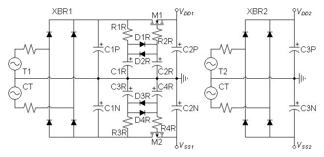 |
SPICE shows IVDD1 = 169mA and IVSS1 = 182mA, assume both could vary with a maximum of 200mA. Design to 1V ripple at regulator input.
| (6) |
C1P = | i
fΔv |
= |
200mA
120Hz × 1V |
= 1.66667mF |
If the raw VDD1 and VSS1 supply are used to supply the regulators for two channels double the value and round up to 4.7mF.
If R1R is chosen to be 1kΩ, calculate C1R to reduce ripple seen at input of diode filter to 25mV.
| (7) |
fRC = fripple × | vfiltered-ripple
vripple |
= 120Hz × |
25mV
1V |
= 3Hz |
| (8) |
C1R = |
1
2πfR |
= |
1
2π × 3Hz × 1kΩ |
= 106.103µF |
From datasheet and SPICE model, I estimate the impedance of the filter diodes with a signal of 25mV to be >196MΩ. Since their operating resistance of filter is so high choose C2R arbitrarily.
C2R = 10µF
Choose gate resistor
R2R = 100Ω
I used the TF analysis of SPICE to get output impedance representing that of M1 and M2 without effect of C2P and C2N..
ZVDD1 = 2.68632Ω
ZVSS1 = 1.7812Ω
If C2P and C2N are desired to bypass the transfer curves of the regulators M1 and M2, I thought to calculate their values for a pole of 20Hz or lower assuming that the feedback factor in the amplifier will reduce if further at that frequency. Use worst case of ZVSS1.
| (9) |
C2N = |
1
2πfR |
= |
1
2π × 20Hz × 1.7812Ω |
= 4.46762mF |
Initially transformer T2 was chosen at 48VCT to meet the power specifications. Since the new design goal was to reduce hum the second transformer could not ride the first piggyback and was separated. Then the value of T1 was raised to 70VCT after the regulators were verified to allow predrivers to drive output MOSFETs to clipping to as close to VDD2 and VSS2 as possible.
To measure the hum this circuit was designed to reduce do a transient and Fourier analysis at 120Hz and calculate total.
Fourier analysis for vdd1:
No. Harmonics: 10, THD: 71.5238 %, Gridsize: 200, Interpolation Degree: 1
| Harmonic | Frequency | Magnitude | |
Phase | |
Norm. Mag | |
Norm. Phase |
|
|
|
|
|
|
|
|||
| 0 | 0 | 0 | 0 | 0 | 0 | |||
| 1 | 120 | 9.78238e-006 | 90.3868 | 1 | 0 | |||
| 2 | 240 | 4.70278e-006 | 92.1464 | 0.48074 | 1.75963 | |||
| 3 | 360 | 3.24187e-006 | 92.5358 | 0.331399 | 2.14902 | |||
| 4 | 480 | 2.36656e-006 | 93.605 | 0.241921 | 3.21826 | |||
| 5 | 600 | 1.93237e-006 | 94.4977 | 0.197536 | 4.11092 | |||
| 6 | 720 | 1.58949e-006 | 95.3495 | 0.162485 | 4.96269 | |||
| 7 | 840 | 1.37518e-006 | 96.3245 | 0.140578 | 5.93777 | |||
| 8 | 960 | 1.19909e-006 | 97.158 | 0.122577 | 6.77119 | |||
| 9 | 1080 | 1.06692e-006 | 98.1152 | 0.109065 | 7.72844 |
Calculate total hum voltage from Fourier data.
| (10) |
vhum-total = vhum-120Hz
× (1 + THD) = 9.78238µV × |
 |
1 + | 71.5238%
100% |
 |
= 16.7791µV |
Calculate decibel hum relative to 1W level (2.82843V into 8Ω) for relevance to speaker sensitivity
| (11) |
dBhum = 20 × log | |
16.7791µV
2.82843V |
|
= -104.536dB |
The calculation for the hum on VSS1 produces nearly identical results.
SPICE Model of standalone power supply setup for hum analysis.
The astute reader might ask why hum had been reduced only modestly after talking about the diode filter eliminating hum. This expectation only applies to the voltage applied to the gate of the MOSFET. The hum that results is a factor of an ac drain to source leakage resistance (rds) in the hundreds of kΩ limiting the ability of the MOSFET to completely eliminate the hum in a non-feedback regulator.
Amplifier Calculations and Simulation Based on New Power Supply
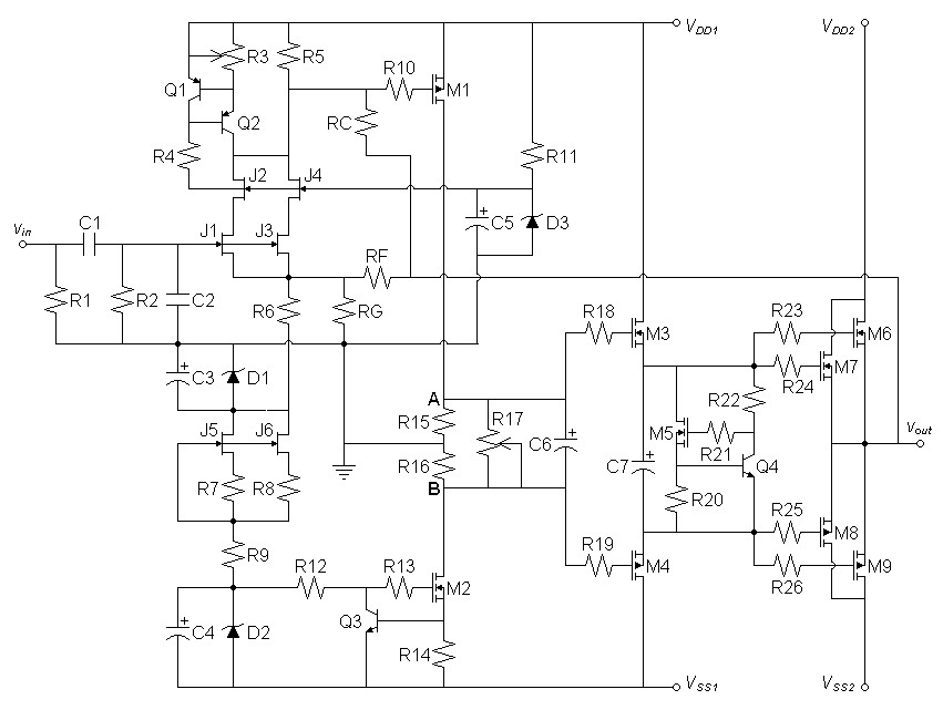
| Figure 4: One-Bend Amplifier of part 3 used to evaluate new power supply. |
 |
Fourier analysis for vout:
No. Harmonics: 16, THD: 73.9737 %, Gridsize: 200, Interpolation Degree: 3
| Harmonic | Frequency | Magnitude | |
Phase | |
Norm. Mag | |
Norm. Phase |
|
|
|
|
|
|
|
|||
| 0 | 0 | 0 | 0 | 0 | 0 | |||
| 1 | 120 | 7.35694e-007 | -90.352 | 1 | 0 | |||
| 2 | 240 | 3.50513e-007 | -86.723 | 0.476439 | 3.62866 | |||
| 3 | 360 | 2.45267e-007 | -88.138 | 0.333382 | 2.21388 | |||
| 4 | 480 | 1.77279e-007 | -86.203 | 0.240968 | 4.14873 | |||
| 5 | 600 | 1.44661e-007 | -85.272 | 0.196632 | 5.08042 | |||
| 6 | 720 | 1.1996e-007 | -84.859 | 0.163057 | 5.49244 | |||
| 7 | 840 | 1.03007e-007 | -83.545 | 0.140014 | 6.80699 | |||
| 8 | 960 | 8.98178e-008 | -82.893 | 0.122086 | 7.45894 | |||
| 9 | 1080 | 8.02879e-008 | -81.829 | 0.109132 | 8.52283 | |||
| 10 | 1200 | 7.23776e-008 | -80.99 | 0.0983799 | 9.36166 | |||
| 11 | 1320 | 6.53764e-008 | -80.166 | 0.0888635 | 10.1863 | |||
| 12 | 1440 | 6.05716e-008 | -79.155 | 0.0823326 | 11.1972 | |||
| 13 | 1560 | 5.54925e-008 | -78.23 | 0.0754288 | 12.1215 | |||
| 14 | 1680 | 5.18678e-008 | -77.512 | 0.0705019 | 12.8395 | |||
| 15 | 1800 | 4.83759e-008 | -76.464 | 0.0657555 | 13.8882 |
Calculate total hum voltage from Fourier data.
| (12) |
vhum-total = vhum-120Hz
× (1 + THD) = 735.694nV × |
|
1 + | 73.9737%
100% |
|
= 1.27991µV |
Calculate decibel hum relative to 1W level (2.82843V into 8Ω) for relevance to speaker sensitivity
| (13) |
dBhum = 20 × log | |
1.27991µV
2.82843V |
|
= -126.887dB |
This value of hum will not be heard with speakers of any known sensitivity.
A quick look at other SPICE results suggest amplifier performing substantially as in third article except for hum improvement.
SPICE model of amplifier
SPICE model of power supply setup to include in the amplifier model
Recommended Amplifier Improvement
I recommend that an actual prototype of the amplifier add a coupling
capacitor in series with inner feedback resistor RC to give
a subsonic zero. This will improve DC offset at the output in two
ways:- By reducing offset drift with power supply voltage variation.
- By removing DC from inner feedback loop, full DC gain works with global feedback for greatest reduction in DC offset.
For RC of 100kHz and a highpass zero of 1Hz this capacitor calculates:
| (14) |
CIFB = |
1
2πfR |
= |
1
2π × 1Hz × 100kΩ |
= 1.59155µF |
Links
Previous articles in this series:- One-Bend Amplifier January 31, 2012. Part 1: Compare a current-feedback amplifier allowing a one-bend distortion characteristic to its voltage-feedback equivalent. Updated March 14, 2012 Added correction concerning output stage transconductance factor and added a link to the next article.
- One-Bend Amplifier March 14, 2012. Part 2: Improving important details of a current-feedback amplifier.
- One-Bend Amplifier June 6, 2012. Part 3: Modified circuit adds a predriver stage.
|
|
Document History
July 7, 2012 Created.
July 7, 2012 Corrected wrong value after equation 14 and added
some additional text.
July 8, 2012 Added comment about the MOSFET's limited hum
suppression capability after equation 11.