 |
| Home │ Audio
Home Page |
Copyright © 2011 by Wayne Stegall
Updated March 3, 2012. See Document History at end for
details.
Cascode Phono Preamplifiers
Introduction
Investigation of a preamp illustrating a low-noise application of the inverting RIAA equalization circuit lead to this discrete preamp design. Although it appears to be a two stage circuit with a buffer, the second stage is only a cascode to the first stage, creating a virtual one-stage design. Separating the class-a input from the cascode with a capacitor enables separate biasing for each. Thus the cascode can have a lower current bias than the input enabling the necessary gain from one stage without excessively high voltage supplies. A direct cascode design would require a power supply in excess of 200V. I investigated two variations on the circuit that did not produce results as good as this one. One was a direct cascode with a shunt resistor around the cascode to the positive supply to reduce cascode bias, resulting in higher distortion. The other was a direct cascode with a shunt current source around the cascode to the positive supply to reduce cascode bias, resulting in lower distortion with higher noise. Both of these had more sensitive and difficult to adjust bias issues. This one turned out simpler in the end.Discrete Circuit
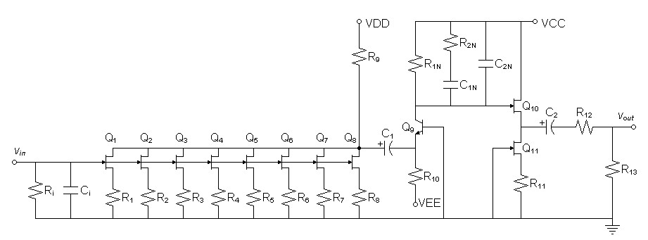
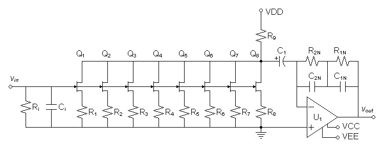
| Figure
1:
Schematic
of
Passive
Cascode
Phono
Preamplifier |
|||||||||||||||||||||||||||||||||||||||||||||||||||||||
 |
|||||||||||||||||||||||||||||||||||||||||||||||||||||||
|
|||||||||||||||||||||||||||||||||||||||||||||||||||||||
| Notes: 1Values calculated for your cartidge can be substituted for default values shown. 2The actual hardware circuit may require hand choosing R9 for the correct VD bias due to JFET parameter variations. 3SPICE simulation showed no significant noise improvement by upgrading to an ultralow noise BJT (i.e. MAT02) because gain falls entirely to input stage. 4A-B capacitor pairs are connected together in parallel. |
Initial Design Decisions
Choose +30V supplies for VDD and VCC. choose -15V supply for VEE.Want gain of 46dB at 1kHz to amplify 5mV to 1Vrms.
Design
Transconductance Front-end Design
It is desirable to choose source resistors small enough to make their noise contribution insignificant compared to the JFET to lower noise.| (1) |
Resistor
noise
equation
(per
√Hz, figure of merit,
does not account for
bandwidth) |
||||
|
| (2) |
R = |
vn-resistor-rtHz2
4kT |
= |
1nV2
4 x 1.3806504e-23 x 298.15ºK |
= 60.7325Ω |
R1-R8 = 27.4Ω
| Figure 2: LSK170A SPICE model for reference |
| .MODEL LSK170A NJF + BETA = 0.0378643 VTO = -0.4025156 LAMBDA = 4.783719E-3 + IS = 3.55773E-14 + RD = 10.6565 RS = 6.8790487 + CGD = 3.99E-11 CGS = 4.06518E-11 + PB = 0.981382 FC = 0.5 + KF = 0 AF = 1 |
It is possible to calculate a gate voltage bias from a drain current specification, but iteration (repetitive computer calculations) or a load line graph are required to calculate the current bias from a specified gate voltage bias. To begin small signal analysis from the parameters given (VGS = 0V and RS = 27.4Ω), get current bias from preliminary SPICE deck.
SPICE shows a combined drain current of 26.3811mA. Individual drain current then calculates to 3.29764mA.
Calculate JFET transconductance:
| (3) |
gfs = 2 × |
|
= 2 × |
|
= 22.3484mS |
Calculate transconductance of individual parallel elements then of entire circuit front-end:
| (4) |
gfs-ckt-element = |
1
RS + 1/gfs |
= |
1
27.4Ω + 1/22.3484mS |
= 13.8608mS |
| (5) |
gfs-front-end = 8 × 13.8608mS = 110.886mS |
Because this stage will drive a cascode through C1, there will be only a trace of AC at VD and therefore no headroom requirement. Because higher values of R9 and R10 will lower distortion as regards the ac impedance seen by the emitter of Q9, choose VD bias at 10V to maximize R9, and calculate R9.
| (6) |
R9 = |
VDD - VD
ID-TOTAL |
= |
30V - 10V
26.3811mA |
= 758.119Ω |
R9 = 750Ω
Calculate C1 for a pole of 0.1Hz
| (7) |
C2 = |
1
2π × R9 × fhp |
= |
1
2π × 750Ω × 0.1Hz |
= 2.12207mF |
C2 = 2200µF
Cascode Design
Calculate DC gain for the desired 46dB gain at 1kHz.| (8) |
AV-DC = 9.89808 × AV-1kHz = 9.89808 × 200V/V = 1979.62V/V |
Given AV-DC = gfs-front-end × R1N calculate R1N for chosen gain.
| (9) |
R1N = |
AV-DC
gfs-front-end |
= |
1979.62V/V
110.886mS |
= 17.8527kΩ |
R10 has two effects on distortion: As pertains to bias, lowering R10 will lower distortion by increasing the bias. As pertains to ac impedance, the parallel of R9 and R10 lower distortion as they are raised. Because R9 is much lower than the expected R10, prefer to choose R10 to increase bias relative to other factors. Choose VC bias at 10V as a compromise between a low R10 and reasonable headroom, and calculate R10.
| (10) |
R10 = |
R1N × VR10
VR1N |
= |
17.8527kΩ(-0.7V - -15V)
(30V - 10V) |
= 12.7647kΩ |
R10 = 13kΩ
Output Buffer Design
The choice of JFET in the output buffer stage is not critical. As for noise the gain stages have amplified their noise enough to make that of the output less critical. Consider that 1nV/√Hz amplified by about 100 gain at 1kHz is 100nV/√Hz. A common 2N3819 would be a good choice as would others in this respect. It is better to prioritize the maximization of gfs in order to reduce buffer stage distortion. To this end, an LSK170 would be a best known choice due to high kn and gfs, with the lowest possible noise for a bonus. Since you would be faced with component variations on a part of your own choice, I suggest you choose a value of R11 by trial and error to get a bias current within your JFETs specifications. You should not match Q10 and Q11. Rather, because Q10 will operate freer if it is not pushed to its current limit, you should choose Q10 to have a higher gfs than Q11. To this end, try both transistors in the Q11 position and place the one there that gives the lowest bias current through Q11. Since this aspect is experimental, calculating R11 may be overengineering. A R11 corresponding to the JFET's rated gfs would be a good starting point for a midpoint bias, i.e.:| (11) |
R11 = |
1
gfs |
= |
1
10mS |
= 50Ω |
| (12) |
R11 = |
|VT|
|IDSS| |
= |
2V
20mA |
= 100Ω |
| (13) |
RS = |
VT
- sqrt(ID/kn)
ID |
Choose R12 output limiter for worst case of 10mA maximum gate current and 20mA maximum drain current.
| (14) |
R12 = |
VCC
IS-MAX |
= |
30V
30mA |
= 1kΩ |
Calculate output coupling capacitor to give 1Hz highpass pole with a 600Ω load knowing that the pole frequency will be much lower with a more reasonable load of 10kΩ:
| (15) |
C2 = |
1
2π × RL-MIN × fhp |
= |
1
2π × (1kΩ + 600Ω) × 1Hz |
= 99.4718µF |
RIAA Analysis
Because the preliminary SPICE deck produced excellent frequency response, I left stray impedances out of the calculations.These calculations are carried out according to the document Phono Equalization Calculations: Passive RIAA Network.
Given R1N = 17.8527kΩ, Calculate R2N.
| (16) |
R2N = |
R1N
6.877358491 |
= |
17.8527kΩ
6.877358491 |
= 2.59587kΩ |
Calculate C1N and C2N from R1N.
| (17) |
C1N = |
2187µs
R1N |
= |
2187µs
17.8527kΩ |
= 122.502nF |
| (18) |
C2N = |
750µs
R1N |
= |
750µs
17.8527kΩ |
= 42.0105nF |
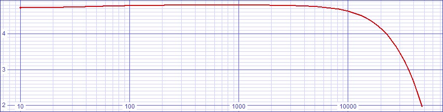
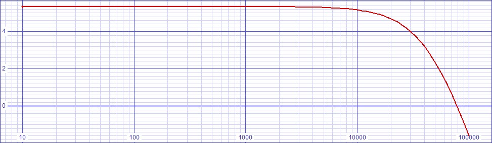
These equalization calculations produce the following plot in SPICE where the response is down to -0.578dB at 20kHz after a 0.07dB rise in the midrange.
| Figure
3:
SPICE
Bode
Plot
of
Discrete
Circuit
with
Initial
Values |
 |
SPICE deck for discrete circuit with inital values.
Supporting models: lsk170.txt, models1.txt, mat02_03.txt, invriaa2.txt.
Adjustments to Discrete Circuit
Standard value component choices produce the following plot where the
response trends generally down to -0.784dB at 20kHz. The standard
values producing this response are logged in the parts list above.| Figure
4:
SPICE
Bode
Plot
of
Discrete
Circuit
after
Standard
Value
Choices |
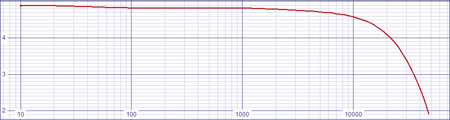 |
The actual hardware circuit may require hand choosing R9 for the correct VD bias due to JFET parameter variations. The bias on the cascode will not require adjustment because BJT voltage bias is accurately predictable.
SPICE deck for discrete circuit with standard value choices.
Supporting models: lsk170.txt, models1.txt, mat02_03.txt, invriaa2.txt.
Other Spice Results
S/N ratio is 104.415dB relative to 1VRMS output.Add 4.71685dB for gain over RIAA for normalized S/N of 109.13185dB
Fourier analysis for vout is dominated by second harmonic:
No. Harmonics: 16, THD: 0.552496 %, Gridsize: 1024, Interpolation Degree: 3
| Harmonic | Frequency | Magnitude | Norm.Mag | Percent | Decibels |
|
|
|
|
|
|
|
| 1 | 1000 | 1.24009 | 1 | 100 | 0 |
| 2 | 2000 | 0.00656276 | 0.00529215 | 0.529215 | -45.52735709 |
| 3 | 3000 | 0.00151543 | 0.00122202 | 0.122202 | -58.25843372 |
| 4 | 4000 | 0.00079421 | 0.000640444 | 0.0640444 | -63.87037677 |
| 5 | 5000 | 0.000486011 | 0.000391915 | 0.0391915 | -68.13616228 |
| 6 | 6000 | 0.00040426 | 0.000325991 | 0.0325991 | -69.7358878 |
| 7 | 7000 | 0.00035357 | 0.000285115 | 0.0285115 | -70.89959867 |
| 8 | 8000 | 0.000310044 | 0.000250016 | 0.0250016 | -72.04064395 |
| 9 | 9000 | 0.000275186 | 0.000221908 | 0.0221908 | -73.07654081 |
| 10 | 10000 | 0.000247239 | 0.000199371 | 0.0199371 | -74.00676026 |
| 11 | 11000 | 0.000225024 | 0.000181457 | 0.0181457 | -74.82452547 |
| 12 | 12000 | 0.000206485 | 0.000166508 | 0.0166508 | -75.57129791 |
| 13 | 13000 | 0.000190323 | 0.000153475 | 0.0153475 | -76.27924716 |
| 14 | 14000 | 0.000176728 | 0.000142512 | 0.0142512 | -76.9229713 |
| 15 | 15000 | 0.000165178 | 0.000133198 | 0.0133198 | -77.51004592 |
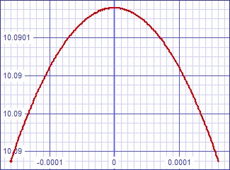
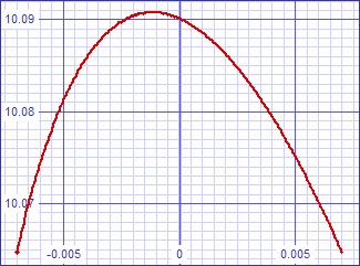
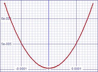
I expect that gain change with frequency will change the way preequalization and postequalization transfer curves juxtapose to create the final transfer curve. Therefore transfer error curve analysis is given for three frequency ranges:
| Figure
x:
Transfer
curve
error
at
DC-50Hz |
Figure x: Transfer curve error at 1kHz | Figure x: Transfer curve error at 21kHz |
 |
 |
 |
I initally attributed an incorrect cause to the fact that all of these curves have a bend direction opposite that of the hybrid circuit because I falsely presumed the hybrid circuit to be inverting as the discrete one. Now I attribute it to this discrepancy.
Hybrid Circuit
| Figure
5:
Schematic
of
Hybrid
Cascode
Phono
Preamplifier |
||||||||||||||||||||||||||||||||||||||||
 |
||||||||||||||||||||||||||||||||||||||||
|
||||||||||||||||||||||||||||||||||||||||
| Notes: 1Values calculated for your cartidge can be substituted for default values shown. 2The actual hardware circuit may require hand choosing R9 for the correct VD bias due to JFET parameter variations. 3A-B capacitor pairs are connected together in parallel. |
This is the circuit that inspired the one above.
Initial Design Decisions
Choose +30V supply for VDD, +15V supply for VCC, and -15V supply for VEE.Want gain of 46dB at 1kHz to amplify 5mV to 1Vrms.
Transconductance Front-end Design
This circuit has the same front-end design as the discrete version. It is only necessary to carry forward the resistance calculated for R1N in the discrete circuit as the DC impedance of the inverting RIAA network used here and do the RIAA Analysis.RIAA Analysis
These calculations are carried out according to the document Phono Equalization Calculations: Inverting RIAA Network.Given R1N + R2N = 17.8527kΩ, Calculate R1N and R2N.
| (19) |
R1N = | 17.8527kΩ × 11.7778
12.7778 |
= 16.4556kΩ |
| (20) |
R2N = | 17.8527kΩ × 1
12.7778 |
= 1.39717kΩ |
| (21) |
C1N = | TP1
R1N |
= |
3180µs
16.4556kΩ |
= 193.247nF |
| (22) |
C2N = | TP2
R2N |
= |
75µs
1.39717kΩ |
= 53.6799nF |
These equalization calculations produce the following plot in SPICE where the response is flat until down to -0.637dB at 20kHz
| Figure
6:
SPICE
Bode
Plot
of
Hybrid
Circuit
with
Initial
Values |
 |
SPICE deck for hybrid circuit with inital values.
Supporting models: lsk170.txt, OPA227.txt, AD797AN.txt, invriaa2.txt.
Adjustments to Hybrid Circuit
Because this circuit places its operational amplifier after first-stage transconductance gain, it seemed that it would not require an ultralow-noise operational amplifier such as an AD797 or a NME49990. After simulating SPICE an AD797 with an ultralow noise spec of 0.9nV/√Hz as a baseline, I first tried an AD825 with an ordinary noise spec of 12nV/√Hz as an alternative because of its 10kHz dominant pole. This combination lost the circuit 1dB of SNR compared to the AD797. I then tried an OPA227 with a low noise spec of 3nV/√Hz as a compromise. Because it simulated essentially the same noise results as the AD797, I chose it as a more cost effective alternative.Standard value component choices produce the following plot where the response is flat until down to -0.657dB at 20kHz. The standard values producing this response are logged in the parts list above.
| Figure
6:
SPICE
Bode
Plot
of
Hybrid
Circuit
after
Standard
Value
Choices |
 |
SPICE deck for hybrid circuit with standard value choices.
Supporting models: lsk170.txt, OPA227.txt, AD797AN.txt, invriaa2.txt.
Other Spice Results
S/N ratio is 1.03896dB relative to 1VRMS output.Add 5.1915dB for gain over RIAA for normalized S/N of 109.088dB
Fourier analysis for vout:
No. Harmonics: 16, THD: 0.148538 %, Gridsize: 1024, Interpolation Degree: 3
| Harmonic | Frequency | Magnitude | Norm.Mag | Percent | Decibels |
|
|
|
|
|
|
|
| 1 | 1000 | 1.30842 | 1 | 100 | 0 |
| 2 | 2000 | 0.00100123 | 0.000765218 | 0.0765218 | -62.32429645 |
| 3 | 3000 | 0.000961284 | 0.00073469 | 0.073469 | -62.67791743 |
| 4 | 4000 | 0.000729173 | 0.000557292 | 0.0557292 | -65.07834383 |
| 5 | 5000 | 0.000576157 | 0.000440345 | 0.0440345 | -67.12413861 |
| 6 | 6000 | 0.000485056 | 0.000370719 | 0.0370719 | -68.6191031 |
| 7 | 7000 | 0.000413432 | 0.000315978 | 0.0315978 | -70.00686308 |
| 8 | 8000 | 0.000363602 | 0.000277894 | 0.0277894 | -71.1224166 |
| 9 | 9000 | 0.000322851 | 0.000246748 | 0.0246748 | -72.15492718 |
| 10 | 10000 | 0.000291564 | 0.000222837 | 0.0222837 | -73.04025394 |
| 11 | 11000 | 0.000264078 | 0.00020183 | 0.020183 | -73.9002856 |
| 12 | 12000 | 0.00024286 | 0.000185613 | 0.0185613 | -74.6278322 |
| 13 | 13000 | 0.000223275 | 0.000170645 | 0.0170645 | -75.35812865 |
| 14 | 14000 | 0.000207823 | 0.000158835 | 0.0158835 | -75.98107585 |
| 15 | 15000 | 0.000194001 | 0.000148271 | 0.0148271 | -76.57887567 |
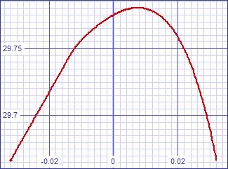
For now I presume that preequalization transfer curve of the JFET front end dominates due to the seemingly vanishing distortion specification of the operational amplifier. Therefore I expect that the low frequency transfer error curve will suffice for the entire audio band:
| Figure x: Transfer curve error at DC-50Hz |
 |
|
|
Document History
May 3, 2011 Created.
May 4, 2011 Added missing × symbol in equation (5), reformatted
equation (1), update figure 5 schematic and revised explanation of R10
choice preceding equation (10).
May 6, 2011 Completed hybrid design promised for second circuit.
May 6, 2011 Updated SPICE decks to replace any unchanged
preliminary
values with correct calculated ones. The differences were not
ones expected to change the results.
May 10, 2011 Corrected two grammar and spelling faults.
May 20, 2011 Improved SPICE decks to reduce interpolation noise
in fourier results.
March 3, 2012 Added transfer error curve analysis for both
circuits. Corrected incorrect interpretation of inverted transfer
error curve bend direction between circuits.