 |
| Home │ Audio
Home Page |
Copyright © 2010 by Wayne Stegall
Updated November 2, 2010. See document history at end.
Musical Feedback Amplifiers
Introduction
I bought my first audio system at the end of the classic audio period. That is, just before integrated circuit operational amplifiers and CD players completely changed the audio market. I first heard of the deficiency when my audio retailer offered to buy back my Nakamichi 480 cassette deck. His rationale was that Nakamichi abandoned discrete amplifiers in their decks in favor of the new op-amps. Many audiophiles were looking to buy their older equipment because it sounded better. Are operational amplifiers that bad? Certainly, they have improved greatly since they first saw use in audio equipment.The Problem
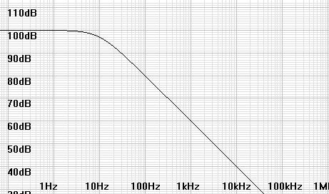
I believe that the common use of dominant-pole compensation in operational amps is the major cause of complaints of sterile or harsh sound on the part of some audiophiles. Many amplifiers have open loop phase shift exceeding 180° before gain drops below unity without some form of compensation. This results in undesirable RF oscillations. Dominant-pole compensation adds extra capacitance to one of the stages to create a lower dominant pole. Then the gain will drop below unity before phase shift gets near enough to 180° to cause oscillations. Consider the following open-loop characteristic of a 741 op-amp, that its response falls 6db/octave (20db/decade) above the dominant pole. This response is typical of many op-amps.Figure 1: Open loop gain of 741 op-amp shows 10Hz dominant pole. |
 |
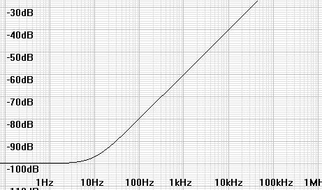
Distortion is typically reduced by the feedback factor (AOL/ACL). Now consider the following distortion suppression plot at unity closed-loop gain (ACL = 0dB). Above the dominant pole, the reduction in distortion suppression creates a distortion profile with greater distortion and more of it consisting of high numbered harmonics. This is contrary to musical and euphonic distortion profiles that fall quickly with harmonic number.
Figure 2: Distortion suppression diminishes 6db/octave above the dominant pole frequency. |
 |
The Solution
One could always revert to single stage amplifiers which never approach 180° phase shift. A three stage amplifier like the 741 would always approach an uncompensated phase shift of at least 270°. Two stage amplifiers ideally would approach 180° phase shift, but reality dictates they may require compensation as well. In any case, if the dominant pole could be made greater than 10kHz-11kHz, the distortion profile would be much flatter than in the above diagram.In the case of the three stage amplifier, if one had access to the compensation terminals or the design was discrete, gain could be sacrified for a higher dominant pole frequency. This would amount to 40db of gain out to 10kHz for a 741. The amplifier would have more distortion but perhaps that more agreeable to some audiophiles (An open loop distortion of 10% would be reduced by feedback to 0.1%). Op-amps with greater gain-bandwidth products would produce better overall results than this example.
Another tweek is a matter of preference. Symmetrical circuit designs produce odd harmonics only. Designing in asymmetry or adding it after the fact can bias the distortion profile back to having a balance of even and odd harmonics. An appropriate-sized resistor or a current source from the output of an amplifier to one of the supply rails can accomplish this. An added benefit is the elimination of crossover distortion by rebiasing the output stage to class A.
Two Stage Amplifier Examples
The following circuits were unstable without compensation according to SPICE1 modeling. With dominant pole compensation of pole frequency >= 20kHz, they showed stable results. I tried poles approaching 100kHz with good results also. Their asymmetrical design should ensure even and odd harmonics for those with that preference.The design for each proceeds as follows:
- Make transistor choices. (I chose LSK170A JFETs and 2N3906 PNPs for these analyses, other choices would work well too.)
- Decide power supply voltages.
- Choose RL (and R1 and R2 if used) for desired output impedance (in this case 1kΩ).
- Choose RBE to set bias through Q1. Check Q1 datasheet for a proper value here.
- Choose CC for desired compensation pole
frequency. (Ordinarily this involves examining the loop gain in
great detail, here SPICE should show whether our pole chosen for
musical reasons will result in oscillation.)
- Calculate maximum possible RS value to choose RS potentiometer value.
- Adjust RS in final circuit to trim offset in output to 0mV.
Output impedance in calculations is open-loop. Closed loop output impedance will be reduced by the feedback factor (AOL/ACL). Adding a small resistance (100Ω-1kΩ) on the output can give short circuit protection where an external cable is driven.
As for the outcomes, all had a declining harmonic profile at 1kHz, the first two emphasizing the second harmonic. That the last emphasized the 3rd, 6th, and 9th relative to the downward trend suggests an unexpected symmetry to the design perhaps due to more direct feedback to the source of the input transistor.
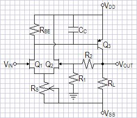
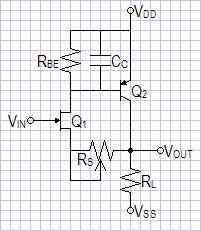
Figure 3: Simplest voltage-feedback op-amp with non-inverting feedback network. |
 |
Choose power supplies as +-15V.
ZOUT = RL || (R1 + R2) = 1kΩ.
Choose RL = 2kΩ, therefore R1 + R2 = 2kΩ.
For gain of 10, R1 = 200Ω, R2 = 1.8kΩ. (Ideal gain formula here is ACL = 1 + R2/R1)
iB-Q3 = -VSS/(hfe x ZOUT) = 15/(100 x 2kΩ) = 75µA.
LSK170A has min IDSS of 2.6mA, choose iD = 2mA and calculate RBE.
RBE = vbe/(iD - iB-Q3) = 700mV/(2mA - 75µA) = 363.6363636Ω.
Round up to nearest standard 5% value: RBE = 360Ω.
rb-Q3 = VT/iB-Q3 = 25mV/75µA = 333.3333333Ω. (VT is the temperature dependent characteristic voltage of a PN junction, usually 25-26mV)
RPOLE = RBE || rb-Q3 = 360Ω || 333.3333333Ω = 173.0769231Ω
| CPOLE = |
1
2πfPOLERPOLE |
= |
1
2π x 20kHz x 173.0769231Ω |
= 45.97809467nF |
CC = CPOLE - Cb, because CPOLE >> Cb, CC (approx.)= CPOLE = 45.97809467nF.
Choose standard value CC = 47nF.
RS-MAX = (|VSS|+|Vp0-MAX|)/(iD x 2) = (15V+2V)/(2 x (700mV/360Ω + 75µA)) = 4.209078404kΩ.
Choose RS = 5kΩ potentiometer.
SPICE results: -3dB @ 721kHz, SNR = 109.9167199dB
Fourier analysis for v(vout) @1V peak:
No. Harmonics: 10, THD: 0.0325317 %, Gridsize: 200, Interpolation Degree: 1
| Harmonic | Frequency | Magnitude | Phase | Norm. Mag | Norm. Phase |
|
|
|
|
|
|
|
| 0 | 0 | 0 | 0 | 0 | 0 |
| 1 | 1000 | 0.998134 | -90.083 | 1 | 0 |
| 2 | 2000 | 0.000322411 | -166.06 | 0.000323014 | -75.972 |
| 3 | 3000 | 1.9347e-005 | -61.106 | 1.93832e-005 | 28.9777 |
| 4 | 4000 | 2.41122e-005 | -161.97 | 2.41573e-005 | -71.882 |
| 5 | 5000 | 9.61602e-006 | -163.8 | 9.63399e-006 | -73.716 |
| 6 | 6000 | 1.99794e-005 | 18.9461 | 2.00168e-005 | 109.029 |
| 7 | 7000 | 2.44962e-006 | 25.7044 | 2.4542e-006 | 115.788 |
| 8 | 8000 | 2.00716e-006 | 105.38 | 2.01091e-006 | 195.463 |
| 9 | 9000 | 5.51143e-006 | -52.899 | 5.52173e-006 | 37.1841 |
SPICE Model for circuit of figure 32.
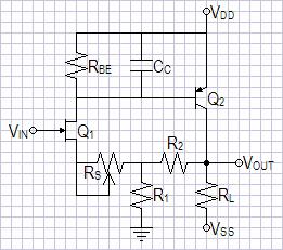
Figure 4: Simplest current-feedback op-amp with non-inverting feedback network. |
 |
The design is the same as the first circuit of figure 3 except you may have to tinker with more values:
ZOUT = RL || (R1 + R2)
Because R1 || R2 sets lower limit for RS trim it was necessary to lower R1 and R2. You may have to rechoose them yourself before recalculating. This will be necessary if you notice that you cannot zero a persistent negative offset. I had forgotten I had made these changes until I examined my SPICE model. ;-)
Choose RL = 2.2kΩ
To get RS to trim I chose, for gain of 10, R1 = 82Ω, R2 = 750Ω. (Ideal gain formula here is ACL = 1 + R2/R1)
ZOUT = RL || (R1 + R2) = 2.2kΩ || (82Ω + 750Ω) = 603.6939314Ω. (Lower than target impedance ok.)
LSK170A has min IDSS of 2.6mA, choose iD = 2mA and calculate RBE.
iB-Q3 = ((|VSS|/ZOUT) - (R1/(R1 + R2))iD)/hfe = (15/2.2kΩ - (82Ω/(82Ω+750Ω))2mA)/100 = 66.21066434µA. (Here R1/(R1 + R2) is the current divider ratio for current through R2)
RBE = vbe/(iD - iB-Q3) = 700mV/(2mA - 66.21066434µA) = 361.9835869Ω.
Round to nearest standard 5% value: RBE = 360Ω.
Rechose RBE = 430Ω to allow zeroing offset voltage in SPICE.
rb-Q3 = VT/iB-Q3 = 25mV/66.21066434µA = 377.5826787Ω. (VT is the temperature dependent characteristic voltage of a PN junction, usually 25-26mV)
RPOLE = RBE || rb-Q3 = 430Ω || 377.5826787Ω = 201.0451142Ω
| CPOLE = |
1
2πfPOLERPOLE |
= |
1
2π x 20kHz x 201.0451142Ω |
= 39.58189776nF |
CC = CPOLE - Cb, because CPOLE >> Cb, CC (approx.)= CPOLE = 39.58189776nF.
Choose standard value CC = 43nF.
RS-MAX = (|Vp0-MAX|)/iD - (R1 || R2) = (2V)/(700mV/430Ω + 66.21066434µA) - (82Ω || 750Ω) = 1.28065872kΩ - 73.91826923Ω = 1.20674045kΩ.
Choose RS = 1.5kΩ potentiometer.
SPICE results: -3dB @ 344kHz, SNR = 111.5468636dB
Fourier analysis for v(vout) @1V peak:
No. Harmonics: 10, THD: 0.141913 %, Gridsize: 200, Interpolation Degree: 1
| Harmonic | Frequency | Magnitude | Phase | Norm. Mag | Norm. Phase |
| -------- | --------- | --------- | ----- | --------- | ----------- |
| 0 | 0 | 0 | 0 | 0 | 0 |
| 1 | 1000 | 0.976102 | -90.179 | 1 | 0 |
| 2 | 2000 | 0.00137924 | -166.68 | 0.001413 | -76.502 |
| 3 | 3000 | 0.00012591 | -70.874 | 0.000128993 | 19.3051 |
| 4 | 4000 | 1.30793e-005 | -165.06 | 1.33996e-005 | -74.884 |
| 5 | 5000 | 9.43717e-006 | -169.82 | 9.66823e-006 | -79.643 |
| 6 | 6000 | 1.94354e-005 | 18.669 | 1.99112e-005 | 108.848 |
| 7 | 7000 | 2.24247e-006 | 24.946 | 2.29737e-006 | 115.125 |
| 8 | 8000 | 1.97063e-006 | 102.57 | 2.01887e-006 | 192.749 |
| 9 | 9000 | 5.60066e-006 | -50.817 | 5.73778e-006 | 39.3625 |
This circuit may require more adjustment than it is worth. The other two are easier to setup and adjust, even in SPICE.
SPICE Model for circuit of figure 42.
Figure 5: Simplest current-feedback op-amp buffer. |
 |
The design is the same as the first circuit of figure 3 except for a few changes:
Choose power supplies as +-15V.
ZOUT = RL = 1kΩ.
LSK170A has min IDSS of 2.6mA, choose iD = 2mA and calculate RBE.
iB-Q3 = ((|VSS|/ZOUT) - iD)/hfe = (15/1kΩ - 2mA)/100 = 130µA.
RBE = vbe/(iD - iB-Q3) = 700mV/(2mA - 130µA) = 374.3315508Ω.
Round up to nearest standard 5% value: RBE = 390Ω.
rb-Q3 = VT/iB-Q3 = 25mV/130µA = 192.3076923Ω. (VT is the temperature dependent characteristic voltage of a PN junction, usually 25-26mV)
RPOLE = RBE || rb-Q3 = 390Ω || 192.3076923Ω = 128.7978864Ω
| CPOLE = |
1
2πfPOLERPOLE |
= |
1
2π x 20kHz x 128.7978864Ω |
= 61.78476509nF |
CC = CPOLE - Cb, because CPOLE >> Cb, CC (approx.)= CPOLE = 61.78476509nF.
Choose standard value CC = 68nF.
RS-MAX = (|Vp0-MAX|)/iD = (2V)/(700mV/390Ω + 130µA) = 1.039030238kΩ.
Choose RS = 1.5kΩ potentiometer (Perhaps it is close enough to try 1kΩ).
SPICE results: -1dB @ 1MHz, -3dB @ 68.6MHz, SNR = 131.9213464dB
Fourier analysis for v(vout) @1V peak:
No. Harmonics: 10, THD: 0.00345022 %, Gridsize: 200, Interpolation Degree: 1
| Harmonic | Frequency | Magnitude | Phase | Norm. Mag | Norm. Phase |
| -------- | --------- | --------- | ----- | --------- | ----------- |
| 0 | 0 | 0 | 0 | 0 | 0 |
| 1 | 1000 | 0.997805 | -90.009 | 1 | 0 |
| 2 | 2000 | 3.83964e-006 | -117.93 | 3.84809e-006 | -27.921 |
| 3 | 3000 | 4.24798e-006 | 10.7399 | 4.25733e-006 | 100.749 |
| 4 | 4000 | 2.49325e-005 | -162.05 | 2.49874e-005 | -72.043 |
| 5 | 5000 | 9.3969e-006 | -163.01 | 9.41758e-006 | -72.998 |
| 6 | 6000 | 1.99808e-005 | 18.7056 | 2.00247e-005 | 108.715 |
| 7 | 7000 | 2.29573e-006 | 29.9847 | 2.30078e-006 | 119.994 |
| 8 | 8000 | 2.14031e-006 | 103.064 | 2.14502e-006 | 193.073 |
| 9 | 9000 | 5.77758e-006 | -50.415 | 5.79029e-006 | 39.5944 |
SPICE Model for circuit of figure 52.
Possibly Musical IC Operational Amplifiers3
Amplifiers with dominant pole >= 10kHz created by wide bandwidth and somewhat lowish open loop gain. Others have claimed excellent sound from them. Their wide bandwidth will require physically short feedback paths.These also have a dominant pole >= 10kHz but I am unaware of any established reputation.
- Analog Devices: AD817 (single), AD825 (single), and AD847 (single).
- Texas Instruments/Burr Brown: OPA690 (single, OPA2690 dual, OPA3690 triple), OPA820 (single, OPA4820 quad), OPA830 (single, OPA2830 dual, OPA4830 quad), OPA2889 (dual), OPA890 (single, OPA2890 dual)
- Texas Instruments THS4021 (Compensation method described in technical document Using a Decompensated Op Amp for Improved Performance)
Others
Some Class AB power amplifiers designed and published by G. Randy Slone have a dominant pole >= 10kHz and were popular while he was selling kits. This objectivist's use of emitter resistors for local feedback in the differential front end is another subjectivist friendly audiophile feature. See his texts to determine which ones.4|
|
1The Spice
Home Page, visit this link learn about using the SPICE simulator
2Links to supporting SPICE models on this
website: LSK170.txt,
models1.txt
3This listing is not intended to be an
endorsement of the products nor is likely complete. Other ICs may
have similar qualities.
4G. Randy Slone, The Audiophile's Project Sourcebook
(New York, 2002), I made this
discovery while looking at his book shortly before this addition.
Document history
April 29, 2010
Created and immediately updated with lower drain bias for examples.
April 30, 2010 Corrected design procedure of circuit of figure 4.
April 30, 2010 Added minor updates.
May 1, 2010 Corrected all design procedures of circuits of
figures 3-5 for faulty bias presumptions and updated SPICE models to
match. Original circuits did simulate in SPICE well.
July 19, 2010 Added SPICE distortion profiles for examples at
1kHz and
a leading comment about them, and a list of Possibly Musical IC
Operational Amplifiers.
September 2, 2010 Added to list of Possibly
Musical IC
Operational Amplifiers and added mention of class AB power amplifiers
meeting this article's criteria.
September 18, 2010 Added link to LM6171
datasheet.
September 21, 2010 Deleted AD823 from list of
op-amps because it
did not match the scope of this article.
November 2, 2010 Added AD847 to list of Possibly
Musical IC
Operational Amplifiers and a link to its datasheet.