 |
| Home │ Audio Home Page |
Copyright © 2011, 2022 by Wayne Stegall
Updated September 26, 2022. See Document History at end
for details.
Local Feedback
Is Local Feedback the same
concept as Global Feedback?
Introduction
The operation of a transistor with respect to the linearizing effect of a source or emitter resistor is so straightforward that it is often difficult to regard its operation as feedback in the same sense as global feedback. Is local feedback the same mechanism as global feedback? It the purpose of this article to examine this question by solving for the closed-loop feedback gain equations of circuits using global feedback and local feedback.Feedback around a voltage gain block
The first circuit to examine applies global feedback to a
differential input voltage gain block. In all these circuits
β represents a numerical value which when multiplied to the output
value gives the voltage applied as feedback. Usually, global
feedback uses a voltage divider and local feedback uses an
impedance to implement β, both usually resistive.| Figure 1: Circuit illustrating global feedback applied to a differential input voltage gain block |
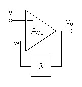 |
Beginning with the open loop gain equation, solve for the closed-loop feedback gain equation.
| (1) |
vo = AOL(vi
- vf) |
| (2) |
vo = AOL(vi - βvo) |
| (3) | vo = AOLvi - AOLβvo |
| (4) | vo + AOLβvo = AOLvi |
| (5) | vo(1 + AOLβ) = AOLvi |
| (6) |
ACL = |
vo
vi |
= |
AOL
1 + AOLβ |
This result is the standard equation defining closed-loop gain for global feedback. This is the reference to which the other equations are compared. All feedback equations of this form (equations (6), (13), and (19)) reduce to
| (7) |
ACL ≈ | 1
β |
Feedback around a transconductance gain block
The second circuit to examine applies global feedback to a
differential input transconductance gain block. This is
useful as an intermediate step because of the similarity to the
transconductance gain of a transistor when feedback is applied.| Figure 2: Circuit illustrating global feedback applied to a differential input transconductance gain block |
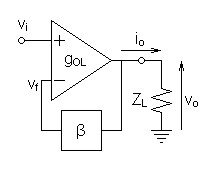 |
Beginning with the open loop gain equation, solve for the closed-loop feedback gain equation. If β is implemented as a voltage divider, its contribution should be added to ZL.
| (8) |
vo = gOLZL(vi
- vf) |
| (9) |
vo = gOLZL(vi - βvo) |
| (10) | vo = gOLZLvi - gOLZLβvo |
| (11) | vo + gOLZLβvo = gOLZLvi |
| (12) | vo(1 + gOLZLβ) = gOLZLvi |
| (13) |
ACL = |
vo
vi |
= |
gOLZL
1 + gOLZLβ |
This result is comparable to the to the standard equation above, except that the output impedance is in the equation. Therefore loading can somewhat affect the gain result if the feedback factor is low.
| > |
Feedback around a transistor gain block
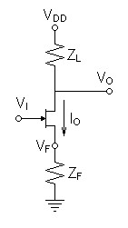
The last circuit to examine is a transistor amplifier with local
feedback. The circuit is meant to represent a generic
transistor although it is illustrated as a JFET, and could
represent a tube circuit as well. The ac equivalent circuit
makes the gate and source or base and emitter effectively
differential inputs. Because the output current also passes
through the inverting input, the feedback impedance ZF
by converting the output current to a feedback voltage at the
feedback terminal becomes the feedback factor β.| Figure
3: Transistor amplifier with local feedback
impedance. |
Figure
4: AC equivalent circuit of same transistor
amplifier |
 |
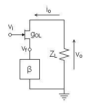 |
Beginning with the open loop gain equation and substituting β for ZF, solve for the closed-loop feedback gain equation.
| (14) |
io = gOL(vi
- vf) |
| (15) |
io = gOL(vi - βio) |
| (16) | io = gOLvi - gOLβio |
| (17) | io + gOLβio = gOLvi |
| (18) | io(1 + gOLβ) = gOLvi |
The resulting closed-loop transconductance gain equation is in the same mathematical form as to standard feedback gain equation of equation (6) above.
| (19) |
gOL = |
io
vi |
= |
gOL
1 + gOLβ |
where vo = ZLio, multiplying the closed-loop transconductance gain equation by ZL gives the closed-loop voltage gain.
| (20) |
AOL = |
vo
vi |
= |
gOLZL
1 + gOLβ |
dividing numerator and denominator by gOL and substituting back ZF for β gives the generic form of the most recognized common-emitter/common-source gain equation:
| (21) |
AOL = |
vo
vi |
= |
ZL
ZF + 1/gOL |
Local feedback calculations take the same form as global ones and even return to the equation most associated with local feedback!
Deductions
Having determined that the mechanism of local feedback is the same as that of global feedback, the differences attributed between them must pertain to differences in their open-loop gain blocks. Individual transistors have comparatively low gain, a one-bend transfer curve, a very high frequency lowpass pole, minimal phase shift of about 90º, and a stable phase margin of about 90º. Multiple transistor gain blocks have high gain, a more complicated transfer curve, and a lowpass pole greatly lowered by the necessity to compensate for 90º or more of phase shift per stage. The following table summarizes these differences and others and their significance.Gain Block Comparison
| Characteristic |
Multiple
Transistor
Gain Block |
Single
Transistor Gain Block |
Winner |
Comments |
| Open-loop Gain (AOL
and gOL) |
high |
low |
multiple transistor |
Many of the multiple
transistor gain block's faults are mitigated here by the
high feedback factor (1 + AOLβ) that results
from high open-loop gain. |
| Transfer Curve1 |
possibly complicated |
one bend |
single transistor |
See first comment. |
| Distortion |
low to vanishing |
high to low |
? |
There may be virtue in
multiple transistor gain block distortion when vanishingly
low, however anything even slightly audible favors the
euphony characteristic of a single transistor gain
block. Still a matter of debate. |
| Output Impedance |
low to vanishing | high to low | multiple transistor? | Low output impedance is
usually a virtue, but not always. |
| Lowpass Pole |
lower, compromised by phase
compensation |
very high |
single transistor |
The multiple transistor
gain block's disadvantage here may be mitigated by
increasing gain bandwidth and possibly decreasing gain
until the dominant pole is 10kHz or higher.2 |
| Compensation Required |
yes |
no |
single transistor |
|
| Maximum Phase Shift before
Compensation |
≈ number_of_stages × 90º | ≈ 90º | single transistor |
|
| Compensated Phase Margin
(180º - Phase Shift at unity open-loop gain) |
≈ 45º | ≈ 90º | single transistor |
This factor relates to
stability: 90º is associated with highest stability, 45º
is associated with a small amount of ultrasonic overshoot
and ringing on transients. |
| Direct Coupling |
yes |
no |
multiple transistor |
Final Comment
I still hold out hope that operational amplifiers could gain virtue by attaining some charactistics of a single transistor, especially those of wide bandwidth and of a high frequency lowpass pole.|
|
1See article Transfer Curve
Shape and Distortion.
2See article Musical Feedback
Amplifiers.
Document
History
August 27, 2011 Created.
September 26, 2022 Correct Compensated Phase Margin in
chart where values transposed.