 |
| Home │ Audio
Home Page |
Copyright © 2010, 2011 by Wayne Stegall
Updated March 26, 2011. See Document History at end for
details.
Low-noise
Hybrid
Op-amp/Discrete
Phono
Preamp
Introduction
Desiring to present a RIAA equalization design example using an operational amplifier, it seems natural to prefer the part with the lowest known noise specification. Analog Devices AD797 is probably the first device to mind with this qualification. This part, however, has a dominant pole of about 7.4Hz. However, its enormous gain and wide bandwidth reduce distortion to levels well below those thought to be audible regardless of the preceding pole specification. That some say it has a excellent but dark sound is additional confirmation of complete lack of audible distortion. Because I wanted to have a switchable extra 50kHz zero, I chose the required output buffer following this function to be discrete. The current-source-biased source-follower buffer is a very low distortion circuit, which I want to add a neutral euphonic distortion profile. The capacitor is not a detriment in this circuit because it would likely have been needed even with an op-amp output buffer. This is because the 60dB DC gain and class-a pull up resistor of the first stage would have produced a good bit more offset than a low gain op-amp application. A capacitor or a dc servo would have been desired regardless. This circuit also benefits because an operational amplifier RIAA circuit simplifies setting gain and equalization compared to a discrete circuit with its transistor variations and stray impedances.
The schematic and SPICE analyses were created with a limited version of National Instrument's MultiSim offered by Analog Devices to evaluate their products. As such, all parts available in the program were either Analog Devices components or enough generic parts needed to complete a design. I maxed the parts count in the schematic below. Therefore, I could not show paralled standard value capacitors separately.
Theory of operation
Operational amplifier U1 and its feedback circuit amplify and equalize the input signal to RIAA specifications adding an extra 50kHz zero. R4 and C4 create a 50kHz pole which switch S1 will use to allow or cancel the extra 50kHz zero. The output buffer serves to isolate the RC filter and drive the load. Furthur, the output buffer puts the very high impedance of its JFET's drains between each power supply connection and the signal path. I intend this to create PSRR (power supply rejection ratio) high enough to reduce power supply concerns in this stage.
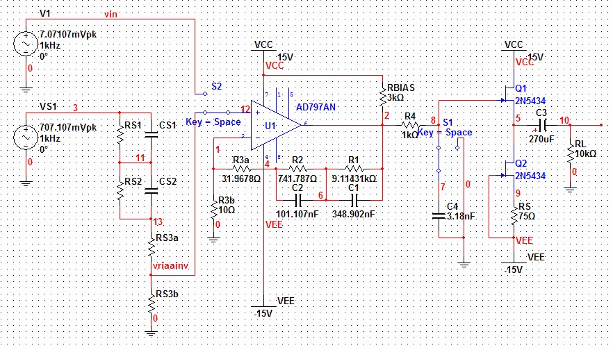
Circuit
| Figure
1:
Schematic
showing
ideal
equalization
values.
Chosen
standard
values
follow
in
parts
list. |
||||||||||||||||||||||||||||||||||||||||||||
 |
||||||||||||||||||||||||||||||||||||||||||||
2This part chosen from limited parts list. I expect you will make substitutions for this part. See design procedure. 3Ri and Ci, are not shown in the circuit, connect them from input to ground. Values calculated for your cartidge can be substituted for default values shown. 4A and b subdesignations of parts indicate parallel combinations meant to serve one part function. 5RL in circuit is altered to test distortion under lowest normal load condition. The actual value is used to properly terminate C3. |
Design Procedure
Calculate RIAA AnalysisSee Calculating Non-inverting RIAA Network with Extra Zero for details and derivation of these calculations.
Choose R3b = 10Ω from AD797 datasheet recommendation.
| (1) |
R3 = |
R3b
0.2382778 |
= |
10Ω
0.2382778 |
= 41.9678Ω |
| (2) |
R3a = R3 - R3b = 41.9678Ω - 10Ω = 31.9678Ω |
| (3) | R2 = R3 × 17.67514356 = 41.9678Ω × 17.67514356 = 741.787Ω |
| (4) | R1 = R3 × 217.173913 = 41.9678Ω × 217.173913 = 9.11431kΩ |
| (5) | C1 = |
TP1
R1 |
= |
3180µs
9.11431kΩ |
= 348.902nF |
| (6) | C2 = |
TP2
R2 |
= |
75µs
741.787Ω |
= 101.107nF |
Now calculate extra-zero switch out circuit:
Choose R4 = 1kΩ and calculate for C4:
| (7) | C4 = | TZ2
R4 |
= |
3.18µs
1kΩ |
= 3.18nF |
Calculate Class-A Biasing
Here the concept is that applying the supply voltage through a voltage divider comprising RBIAS and the lowest load resistance expected should result in a voltage across the load exceeding the maximum expected peak signal. Assuming a minimum load of 10kΩ and a peak signal of 2.828V calculate:
| (8) | RBIAS-MAX = 10kΩ × | 15V - 2.828V
15V |
= 8.11467kΩ |
| (9) | RBIAS-MIN = | 15V
5mA |
= 3kΩ |
| (10) | RBIAS = 3kΩ |
Output Buffer Design
The limits of the trial edition of MultiSim limited my choice of JFET's. It is fortunate then that this choice is not critical. As for noise the op-amp has amplified its noise enough to make that of the output less critical. Consider that 1nV/√Hz amplified by about 100 gain at 1kHz is 100nV/√Hz. A common 2N3819 would be a good choice as would others in this respect. It is better to prioritize the maximization of gfs in order to reduce buffer stage distortion. To this end, an LSK170 would be a best known choice due to high kn and gfs, with the lowest possible noise for a bonus. The best compromise choice given me by MultiSim was a 2N5434 with a kn of 22mA/V2. Even this part is now obsolete. Since you would be faced with component variations on a part of your own choice, I suggest you choose a value of RS by trial and error to get a bias current within your JFETs specifications. You should not match Q1 and Q2. Rather, because Q1 will operate freer if it is not pushed to its current limit, you should choose Q1 to have a higher gfs than Q2. To this end, try both transistors in the Q2 position and place the one there that gives the lowest bias current through Q2. Since this aspect is experimental, calculating RS may be overengineering. A RS corresponding to the JFET's rated gfs would be a good starting point for a midpoint bias, i.e.:
| (11) |
RS = |
1
gfs |
= |
1
17mS |
= 58.8235Ω |
| (12) |
RS = |
|VT|
|IDSS| |
= |
2.5V
30mA |
= 83.3333Ω |
| (13) |
RS = |
VT
- sqrt(ID/kn)
ID |
Calculate output coupling capacitor to give 1Hz highpass pole with a 600Ω load knowing that the pole frequency will be much lower with a more reasonable load of 10kΩ:
| (14) |
C3 = |
1
2π × RL-MIN × fhp |
= |
1
2π × 600Ω × 1Hz |
= 265.2582385µF |
Spice Simulation
SPICE model for ideal circuit.
SPICE model for final circuit.
Magnitude in all Bode plots and Voltage in distortion plots are in units of dB.
| Figure
2:
Bode
and
phase
plots
from
ideal
circuit
before
choosing
standard
values. Cyan plot shows 50kHz zero switched in and magenta plot out. |
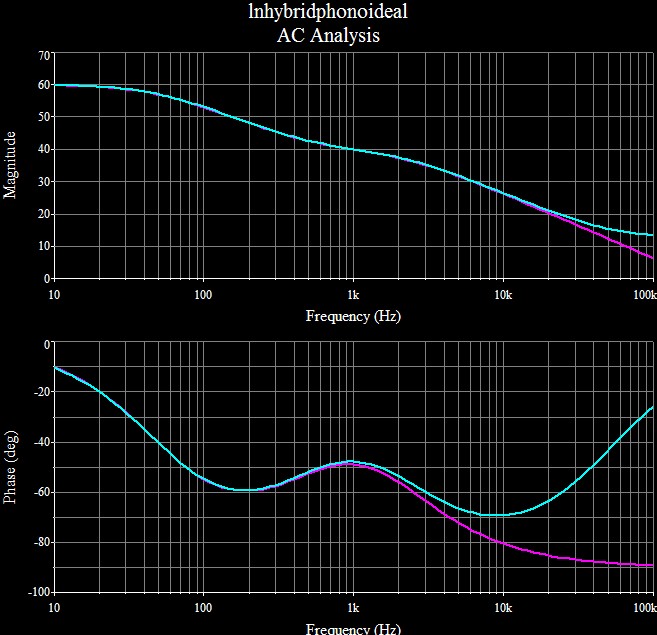 |
Figure 3: Same plots with circuit driven by RIAA inverse preequalizer with extra pole at 50kHz. Cyan plot shows 50kHz zero switched in and magenta plot out. |
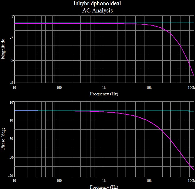 |
Juggle ac analysis in SPICE to choose standard values:
| Figure
4:
Preequalized
bode
plot
with
chosen
standard
values. Cyan plot shows 50kHz zero switched in and magenta plot out. |
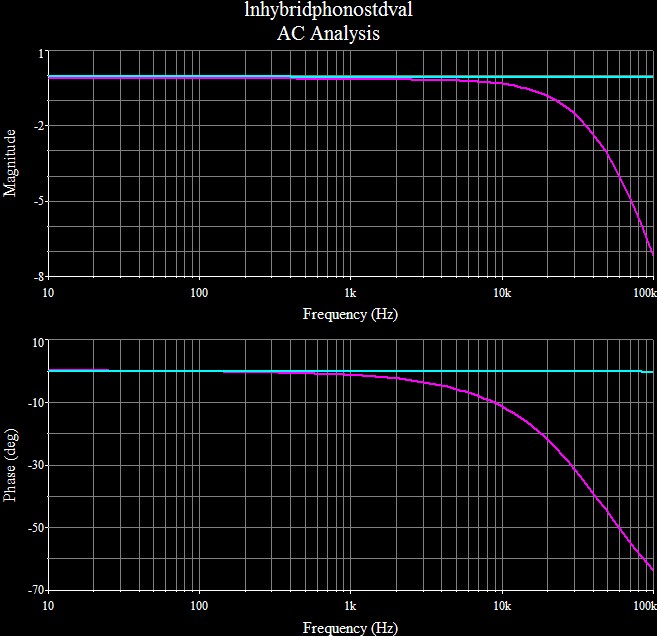 |
All Distortion analyses done with RIAA preequalization to give signal levels the correct frequency balance. Figure 5: Fourier analysis shows harmonic distribution of 0.0022818% distortion of 1kHz signal. Note dominance of second harmonic and to a lesser extent the other even harmonics. |
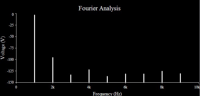 |
Figure 6: 2rd harmonic distortion plot magenta plot shows op-amp distortion rising with frequency and cyan plot shows it masked by frequency-flat distortion profile of output stage. |
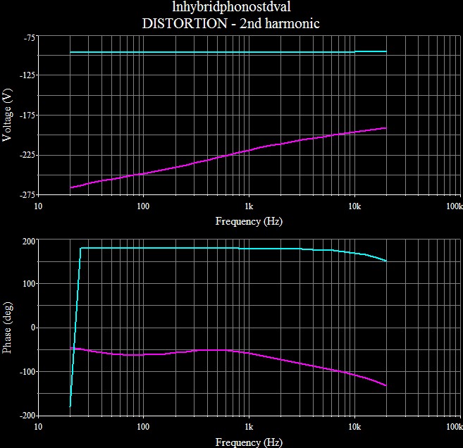 |
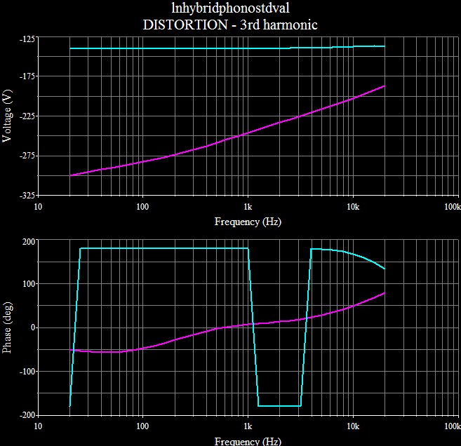
Figure 7: 3rd harmonic distortion plot magenta plot shows op-amp distortion rising with frequency and cyan plot shows it masked by frequency-flat distortion profile of output stage. |
 |
Miscellaneous Spice Results |
| SNR = 99.7334dB relative to 1VRMS
output. AC analyses with ac sources in series with power supplies showed high PSRR in output buffer: PSRR measured 91dB relative to VCC and higher relative to VEE. I did this investigation at the outset to verify my presumptions about the buffer's PSRR and do not remember the second figure exactly. This suggests that a power supply sufficient for the first stage will suffice for the buffer as well. |
Final Comments
Although expected, I was gratified that the distortion results were entirely those of the output buffer, showing little effect by the operational amplifier.|
|
Document History
October 29, 2010 Created.
October 29, 2010 Improved visibility of graphs.
October 30, 2010 Added links to semiconductor datasheets in parts
list.
October 30, 2010 Move class-a bias to connect to positive supply,
and verify no operational changes.
October 31, 2010 Added specific reference to LME79990 as an
alternative op-amp and a link to its datasheet.
January 26, 2011 Made minor symbol improvements.
March 26, 2011 Made minor improvements to text.