 |
| Home │ Audio
Home Page |
Copyright © 2012 by Wayne Stegall
Updated November 3, 2012. See Document History at end for
details.
Warp Filter
Highpass
notch
filter
eliminates
dangerous
LP
warp
signals
Introduction
With 60dB or more of DC gain, a phono preamplifier can amplify record warps into subsonic energy dangerous to woofers. Because of this some proposed long ago to amend the RIAA equalization curve to add a 20Hz highpass pole to filter out subsonics. However this first-order pole will only suppress warp energy by -31.1261dB. The filter circuit proposed here has a second-order pole and a notch at the offending frequency to nearly eliminate the problem altogether.First try
| Figure
1:
Desired
warp
filter
topology |
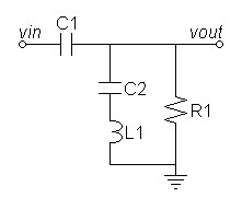 |
Refer to the frequency plot of figure 3 below for the following description. The circuit of figure 1 above operates in the following manner. In the passband above 20Hz C1 passes all signals unaltered. As the frequency drops to near the cutoff frequency, L1 interacts with C1 and R1 to create the usual second-order highpass pole at 15Hz. At this point C2, because of its larger value, only couples L1 with the rest of the circuit. As the response falls due the pole the impedance of c rises as the zero approaches to begin the greater suppression of the notch. When the impedance of C2 becomes equal to that of L1 their opposite polarity results in zero impedance producing the zero magnitude of the notch. Passing the notch the impedance of C2 exceeds that of L1 allowing the magnitude to return to a lower stopband ripple level after which the response drops again in the normal way.
Direct s-domain analysis of circuit produces a third-order transfer curve that does not readily lend itself to a solution.
An empirical solution
It is more desirable then to break the problem down into two
parts. If you can assume that C2 >> C1,
then
C2 can be removed
from the pole analysis allowing separate calculation of pole and
zero. Then the problem reduces to two parts:- Design circuit with C2 removed for desired pole.
- Calculate C2 to give desired zero.
- Simulate and make adjustments if necessary.
Design for pole parameters
| Figure 2: Circuit for pole design |
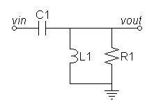 |
First setup and reduce s-domain transfer equation for the simplified circuit:
| (1) |
sL || R |
|
|||||||
| H(s) = |
|
= |
|
||||||
|
|
| (2) |
sLR |
sLR |
|||||
| H(s) = |
|
= |
|
||||
|
|
| (3) |
H(s) = | s2LC1R
s2LC1R + sL + R |
| (4) |
s2 | |||||||
| H(s) = |
|
|||||||
|


Now the fully reduced transfer equation of equation 4 is in the form of the standard second-order highpass transfer curve.
| (5) |
s2 | ||||||
| H(s) = |
|
||||||
|
where the characteristic parameters are derived as follows.
| (6) |
1 |
||
| ω = |
|
||
|
| (7) |
Q
ω |
= C1R, therefore Q = ωC1R |
Combining equations 6 and 7 gives:
| (8) |
C1R | ||
| Q = |
|
||
|
Which reduces to:
| (9) |
Q = R |
|
Desiring a Bessel Q, I determined that fpole for a cutoff of 20Hz is slightly above 15Hz.
Choose 15Hz for pole frequency, then calculate the radian frequency.
| (10) |
ωpole = 15Hz × 2π =
94.2478 radians/s |
The second-order Bessel Q is known as:
| (11) |
1 | |||
| Second order Bessel Q = |
|
≈ 0.57735 |
||
|
Choose R = 100kΩ
Rearrange equation 7 to solve for C1.
| (12) |
C1 = | Q
ωpoleR |
= |
0.57735
94.2478 × 100kΩ |
= 61.2588nF |
C1 = 62nF
Rearrange equation 6 to solve for L:
| (13) |
L = |
1
ωpole2C1 |
= |
1
(94.2478)2 × 62nF |
= 1.81579kH |
Design for zero parameters
Calculate the zero required to cancel a 33⅓ RPM warp:| (14) |
fzero = | 33.3333 cycles/min 60 s/min |
= 0.555555Hz, therefore ωzero = 2π × 0.555555Hz = 3.49066 radians/s |
An equation like equation 6 defines the notch frequency relative to L and C2. Rearrange it and calculate C2.
| (15) |
C2 = |
1
ωzero2L |
= |
1
(3.49066)2 × 1.81579kH |
= 45.198µF |
C2 = 47µF
At this point our initial assumption that C2 >> C1 is correct, validating this shortcut design method.
The necessity to round C2 to the nearest standard value requires recalculation of exact L.
| (16) |
L = |
1
ωzero2C2 |
= |
1
(3.49066)2 × 47µF |
= 1.74617kH |
SPICE results
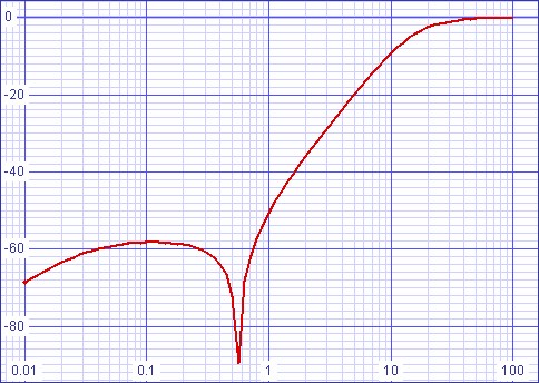
SPICE results verify successful design outcome.SPICE model.
| Figure
3:
Passive
filter
magnitude
response |
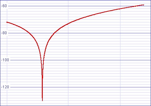
Figure 4: Passive filter phase response |
 |
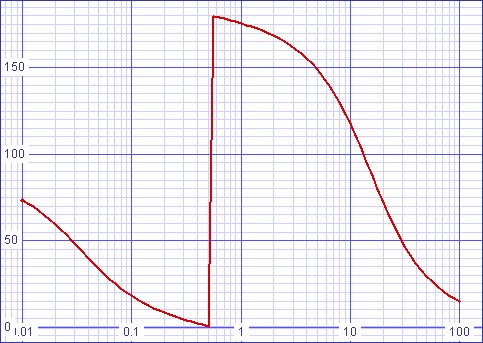 |
Figure 5: Passive filter magnitude notch detail 0.5-0.75Hz |
|
 |
Magnitude response at 0.555555Hz (33⅓ RPM warp) = -165.432dB
Magnitude response at 0.75Hz (45 RPM warp) = -59.288dB
Magnitude response at 20Hz = -2.59905dB.
I did not simulate distortion because it depends on final component choice.
Add active inductor to design
The circuit that follows in figure 5
adds an active inductor consisting
of U1, U2, R1L, R2L, R3L,
C4L, and R5L. It is a form of a circuit
known as a Generalized
Impedance
Converter. Concerns by those who prefer discrete circuits to
operational amplifiers are mitigated by the fact that the active
inductor is only in the signal path in the passband near the resonant
frequency.| Figure 6: Warp filter with active inductor |
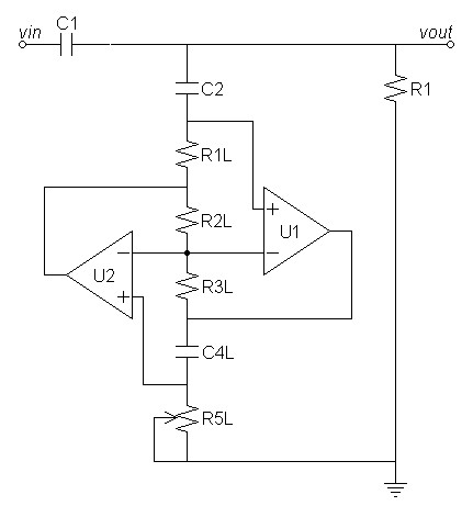 |
The equivalent active inductance is calculated by the formula:
| (17) |
L = |
C4L × R1L ×
R3L × R5L
R2L |
I choose C4L to be 1µF because it is the largest among plastic capacitors to be of reasonable size and price. Then I presume that the resistors would give the best noise result if they were the same values. If all the resistors were set the same in equation 17 above then equation 17 above simplifies to:
| (18) |
L = |
C4L × R1L ×
R1L × R1L
R1L |
= C4L × R1L2 |
Rearrange equation 18 and solve for common resistor value.
| (19) |
R1L = |
|
= |
|
= 41.7872kΩ |
R1L, R2L and R3L = 42.2kΩ
Now restore R5L to equation 18 to calculate its similar adjustable value.
| (20) |
L = |
C4L × R1L ×
R1L × R5L
R1L |
= C4L × R1L × R5L |
Rearrange equation 20 and solve for R5L.
| (21) |
R5L = |
L
C4L × R1L |
= |
1.74617kH
1µF × 42.2kΩ |
= 41.3784kΩ |
SPICE results
Again SPICE results confirm a successful design outcome.SPICE model with active inductor.
| Figure 7: Passive/active filter magnitude response | Figure 8: Passive/active filter phase response |
 |
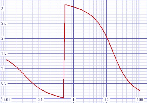 |
Figure 9: Passive/active filter magnitude notch detail 0.5-0.75Hz |
|
 |
Magnitude response at 0.555555Hz (33⅓ RPM warp) = -134.583dB
Magnitude response at 0.75Hz (45 RPM warp) = -59.2881dB
Magnitude response at 20Hz = -2.59943dB.
Because the GIC is supposedly a proven circuit, I used ideal op amps in the simulation.
Application and Adjustments
In actual application, the proper operation of this passive circuit is sensitive to the circuit context into which it is placed. Therefore a buffer should drive it with near zero output impedance and the output should drive near infinite input impedance in the buffer that follows.Adjust R5L to calibrate the correct notch frequency in the manner you see best. I would suspect you would play a warped record at 33⅓ RPM and then
- Measure C2 with an LCR meter and with same meter set l
to the exact value necessary. Depending on the exact C2
value, you may have to recalculate L again as in the equations above.
- Connect an oscilloscope and adjust for the best null or
- Play it carefully through loudspeakers always monitoring for safe volume until the woofer no longer responds to the warp signal.
Generalized
Impedance Converter (GIC)
For those curious about the active inductor itself, I include a little
information about the basis circuit itself.1| Figure
10:
GIC
can
emulate
many
other
impedances
other
than
the
active
inductor |
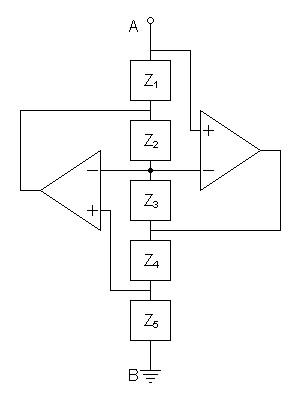 |
Node B is always shown in the source document connected to ground. There is no logical reason to think it has to be this way.
The virtual impedance created by the circuit of figure 10 above is:
| (22) |
ZGIC = |
Z1Z3Z5
Z2Z4 |
|
|
1Arthur B. Williams and Fred J.
Taylor, Electronic Filter Design Handbook (New York, 1988), p. 3-39 -
3-41 "Generalized Impedance Converters."
Document History
September 22, 2012 Created.
September 23, 2012 Made a minor correction just prior to equation
15.
September 25, 2012 Corrected misspellings. I moved quickly
to
publish but I thought I did a spell check.
November 3, 2012 Corrected some grammer.