 |
| Home │ Audio
Home Page |
Copyright © 2013 by Wayne Stegall
Updated April 20, 2015. See
Document History at end for details.
Thermal Design
Part
1:
Thermal design for gainclone and one-bend amplifiers is used to illustrate the presented theory.
Thermal design for gainclone and one-bend amplifiers is used to illustrate the presented theory.
Introduction
For the purposes of managing heat in electronic devices, thermal elements are considered to have a thermal resistance equal to the temperature difference between the two ends of the element divided by the associated flow of heat power. The relation is mathematically equivalent to Ohm's law and therefore allows represent ion and solution of the thermal system as is if it were a resistor network.| (1) |
Thermal Resistance (ºC/W) = | Temperature (ºC) Heat Flow (W) |
Here heat itself would be in units of Joules (J), however the flow of heat would represent power in Watts.
Class B Thermal Design
Calculation of Power Dissipation
Before a thermal design can be done the power dissipated by all the devices feeding into the design heat sink must be calculated.First calculate average output power. Output power is related to rms output voltage and is calculated from peak voltage with a scale factor of ½.
| (2) |
POUT = |
VOUT-PEAK2
2RL |
| (3) |
VOUT-PEAK ≤ VCC – VDO |
Now calculate input power. Because the supply voltages are considered constant, the average power is proportional to the average current. Only the voltage of a single supply is used because apart from a small amount of bias a class b output stage only draws power from one rail of the power supply at a time.
| (4) |
PIN = VCC × IOUT-AVE |
Average current is scaled from peak current by a scale factor of 2/π (≈63.7%).
| (5) |
PIN = VCC |  |
2
π |
IOUT-PEAK |  |
It may be easier to calculate input power from all voltages.
| (6) |
PIN = | 2
π |
× | VCC × VOUT-PEAK
RL |
You may want to calculate the efficiency as well.
| (7) |
Eff = |
POUT
PIN |
= |
|
|||||||||
| (8) |
Eff = | π
4 |
× | VOUT-PEAK
VCC |
Finally power dissipation is just input power minus output power.
| (9) |
PDISS = PIN – POUT = | 2VCC × VOUT-PEAK
πRL |
– | VOUT-PEAK2
2RL |
| (10) |
PDISS = | 4VCC × VOUT-PEAK
– VOUT-PEAK2
2πRL |
Example
Having no class B amplifier design on hand, it seems useful to do the
thermal design of the popular gainclone. The relevant
specifications of the popular LM3886 chip for optimal drive into a 4Ω
load are:| VCC | |
28V |
|
POUT | |
68W |
| TJ-MAX |
150ºC |
RθJC | 1ºC/W |
RθCS = 0.2ºC/W
Given output power, calculate peak output voltage to prepare remaining calculations.
| (11) |
VOUT-PEAK = | 2POUTRL | = |
2 × 68W × 4Ω | = 23.3238V |
Calculate input power.
| (12) |
PIN = | 2
π |
× | VCC × VOUT-PEAK
RL |
= |
2
π |
× | 28V × 23.3238V
4Ω |
= 103.939W |
Finally calculate the power dissipation.
| (13) |
PDISS = PIN – POUT = 103.939W - 68W = 35.9387W |
| Figure
1:
Thermal
circuit representing one semiconductor device mounted
to a heat sink |
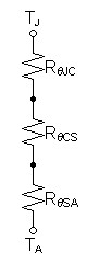 |
For an ambient temperature of 25ºC calculate thermal resistance of desired heat sink.
| (14) |
TJ – TA = PDISSRθJC + PDISSRθCS + PDISSRθSA |
| (15) |
RθSA = | TJ – TA – PDISS(RθJC + RθCS)
PDISS |
| (16) | RθSA = | 150ºC – 25ºC – 35.9387W(1ºC/W +
0.2ºC/W)
35.9387W |
| (17) | RθSA = | 2.27814ºC/W |
Perhaps a presumption of an ambient temperature of 25ºC is too optimistic, try 50ºC (>120ºF).
| (18) | RθSA = | 150ºC – 50ºC – 35.9387W(1ºC/W +
0.2ºC/W)
35.9387W |
| (19) | RθSA = | 1.58252ºC/W |
SPICE Analysis
SPICE model| Figure
2:
SPICE
model of thermal circuit of figure 1 |
| * Thermal circuit
for LM3886 gainclone * SPICE version: Spice Opus 2.31 i1 0 tj dc 35.9387 rthjc tj tc 1 rthcs tc ts 0.2 rthsa ts ta 1.58252 v1 ta 0 dc 25 .end .control op print all .endc |
Figure 3: SPICE output for model of figure 2. |
| ta = 2.500000e+001
tc = 8.906145e+001 tj = 1.250002e+002 ts = 8.187371e+001 v1#branch = 3.593870e+001 |
Class A Thermal Design
Calculation of Power Dissipation
Output power is always calculated the same Therefore the same equation is used here as in the class b calculations| (2) |
POUT = |
VOUT-PEAK2
2RL |
Because transistors operated in class a never turn off the average supply current is always the same as the operating bias current. Unlike with class b input power is independent of output power.
| (20) |
PIN = 2VCC × IBIAS |
It may be useful to calculate input power in terms of voltage rather than bias current.
| (21) |
If IBIAS = |
VOUT-PEAK
2RL-MIN |
| (22) |
PIN = | VCC × VOUT-PEAK
RL-MIN |
Again efficiency calculations may be of interest.
| (23) |
Eff = |
POUT
PIN |
= |
|
|||||||||
| (24) |
Eff = | VOUT-PEAK × RL-MIN
2VCC × RL |
As always the transistors dissipate the input power that does not go to the output.
| (25) |
PDISS = PIN – POUT |
Therefore, a constant input power produces a condition where the transistors dissipate maximum power at a zero output level.
| (26) |
PDISS-MAX = PIN |
and minimum power when the output is at its maximum.
| (27) |
PDISS-MIN = PIN – POUT-MAX |
Example
It seemed that a proper thermal design was a necessary prerequisite to adding a safe-area limiter to the one-bend amp. Although the project was originally conceived only to investigate how to design the transfer curve of an amplifier, I feel compelled to make every aspect of the design correct as time permits.To begin, the IRFP240 and IRFP9240 datasheets give the following thermal data
| PD |
|
150W @ TC = 25ºC | |
TJ | |
–55ºC – 150ºC |
| RθJC | 0.83ºC/W | RθCS | 0.24ºC/W, flat surface with
thermal grease |
First calculate input power.
| (28) |
PIN = 2VCC × IBIAS |
| (29) | PIN = 2 × 35V × 4A |
| (30) | PIN = 280W |
Since the transistors have to dissipate all of the input power at idle, the power calculations are complete.
| (31) |
PDISS = PIN = 280W |
Now calculate for a heat sink protecting four output transistors as in figure 4.
| Figure 4: Thermal circuit representing four semiconductor devices mounted to a heat sink |
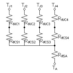 |
First calculate power dissipation required of each transistor.
| (32) |
PDISS/DEVICE = PIN/#devices |
| (33) | PDISS/DEVICE = 280W/4 devices |
| (34) | PDISS/DEVICE = 70W |
Now setup and solve thermal circuit equations for heat sink thermal resistance.
| (35) |
TJ – TA = PDISS/DEVICERθJC1 + PDISS/DEVICERθCS1 + (#devices × PDISS/DEVICE)RθSA |
| (36) |
RθSA = | TJ – TA – PDISS/DEVICE(RθJC1 + RθCS1)
#devices × PDISS/DEVICE |
| (37) | RθSA = | 150ºC – 50ºC – 70W × (0.83ºC/W +
0.24ºC/W)
4 × 70W |
| (38) | RθSA = | 0.0896429ºC/W |
In spite of the fact that four output devices appeared to be able dissipate 280W on first glance, the required heat sink seems unreasonably large especially considering that you would likely choose a larger one for the reliability of a lower junction temperature.
Now recalculate for eight output devices and an ambient temperature of 50ºC.
| Figure 5: Thermal circuit representing eight semiconductor devices mounted to a heat sink |
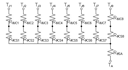 |
First calculate power dissipation required of each transistor.
| (39) |
PDISS/DEVICE = PIN/#devices |
| (40) | PDISS/DEVICE = 280W/8 devices |
| (41) | PDISS/DEVICE = 35W |
Now setup and solve thermal circuit equations for heat sink thermal resistance.
| (42) |
RθSA = | TJ – TA – PDISS/DEVICE(RθJC1 + RθCS)
#devices × PDISS/DEVICE |
| (43) | RθSA = | 150ºC – 50ºC – 35W × (0.83ºC/W +
0.24ºC/W)
8 × 35W |
| (44) | RθSA = | 0.223393ºC/W |
This heat sink value is reasonable, however 0.1ºC/W heat sinks are available and would lower the transistor junction temperature more.
SPICE Analysis
SPICE model| Figure
6:
SPICE
model of thermal circuit of figure 5 |
| * Thermal circuit
for eight transistor class a output stage. * SPICE version: Spice Opus 2.31 i1 0 tj1 dc 35 i2 0 tj2 dc 35 i3 0 tj3 dc 35 i4 0 tj4 dc 35 i5 0 tj5 dc 35 i6 0 tj6 dc 35 i7 0 tj7 dc 35 i8 0 tj8 dc 35 rthjc1 tj1 tc1 0.83 rthcs1 tc1 ts 0.24 rthjc2 tj2 tc2 0.83 rthcs2 tc2 ts 0.24 rthjc3 tj3 tc3 0.83 rthcs3 tc3 ts 0.24 rthjc4 tj4 tc4 0.83 rthcs4 tc4 ts 0.24 rthjc5 tj5 tc5 0.83 rthcs5 tc5 ts 0.24 rthjc6 tj6 tc6 0.83 rthcs6 tc6 ts 0.24 rthjc7 tj7 tc7 0.83 rthcs7 tc7 ts 0.24 rthjc8 tj8 tc8 0.83 rthcs8 tc8 ts 0.24 rthsa ts ta 0.223393 v1 ta 0 dc 25 .end .control op print all .endc |
Figure 7: SPICE output for model of figure 6. |
| ta = 2.500000e+01 tc1 = 9.595004e+01 tc2 = 9.595004e+01 tc3 = 9.595004e+01 tc4 = 9.595004e+01 tc5 = 9.595004e+01 tc6 = 9.595004e+01 tc7 = 9.595004e+01 tc8 = 9.595004e+01 tj1 = 1.250000e+02 tj2 = 1.250000e+02 tj3 = 1.250000e+02 tj4 = 1.250000e+02 tj5 = 1.250000e+02 tj6 = 1.250000e+02 tj7 = 1.250000e+02 tj8 = 1.250000e+02 ts = 8.755004e+01 v1#branch = 2.800000e+02 |
Try this yourself. Alter the SPICE model for a 0.1ºC/W heat sink and note the much lower junction temperature.
|
|
Document History
July 12, 2013 Created.
July 12, 2013 Corrected RθSA in SPICE model of
figure 6, regenerated corresponding SPICE output, and made minor
improvements to wording.
April 20, 2015 Corrected some misspellings.