 |
| Home │ Audio
Home Page |
Copyright © 2011 by Wayne Stegall
Updated April 11, 2011. See Document History at end for
details.
|
|
Managing TIM
Introduction
Although the qualities of an ideal feedback amp have their temptation, subjectivists have convinced me of the virtues of single-ended non-feedback circuits. In low voltage applications where low distortion levels can be achieved by using high bias levels, or where it is otherwise practical, this seems ideal. However, low distortion levels cannot be achieved in power amplifiers without either greatly lowering efficiency or resorting to feedback designs. Also, some signal processing cannot be done practically without the use of op-amps. Therefore, it may become impractical to avoid the use of feedback amplifiers altogether. Because transient intermodulation distortion (TIM) and other frequency limitations are a prime factor in feedback amplifier quality, it would be well to find a way to tame them. TIM is obviously a violation of slew-rate limitations imposed by the open-loop amplifier block. Any attempt to slew the signal faster than the system will allow will distort the signal until the signal comes back within amplifier capabilities. The slew-rate limitation of affected amplifiers is not directly related to gain or bandwidth that its effect could be calculated from a feedback factor. Rather it is a hard limitation like voltage clipping. It would be reasonable to limit signal slew by a chosen or even arbitrary safety factor to avert the problem perhaps in conjunction with listening tests. In effect, what is desired is excess unused bandwidth and slew-rate beyond what the design system requires. Here, analysis is done to determine how to effectively limit signal slew-rate to prevent invoking these limitations.Mathematical Analysis
First derive equations useful to relating bandwidth to slew rate:Begin with the sinusoidal signal model using radian frequency units:
| (1) |
v = vpk sin ωt |
Convert frequency units to Hz:
| (2) |
v = vpk sin 2πft |
Differentiate the equation to get instantaneous slew-rate
| (3) |
dv
dt |
= 2πfvpk cos 2πft |
Take the maximum value as the peak slew-rate:
| (4) |
dv
dt |
(peak) = 2πfvpk = slew
rate |
Now solving for f with respect to slew rate gives an associated bandwidth:
| (5) |
f = |
slew rate
2πvpk |
These equations can either relate signal slew-rate to signal bandwidth or maximum amplifier slew-rate to what is called power bandwidth.
A Practical Solution
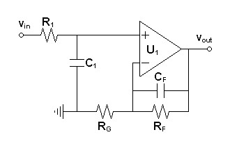
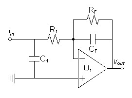
After deriving the power bandwidth, avoiding slew rate problems becomes a matter of limiting the bandwidth of the signal passing to the output of the amplifier. If protecting the amplifier from distortion-producing slew would adversely limit system bandwidth, choosing a wider bandwidth open-loop gain block would also be in order. (I.e. one with greater maximum slew rate.) In the circuit of figure 1 below the RC prefilter formed by R1 and C1 could suffice alone to limit signal slew rate in the amplifier. There is benefit to adding CF in parallel to RF as well. Although the RC feedback pole stops rolling off due to a zero at unity gain, if the open loop gain is rolling off due to a dominant pole with a -90º phase lag the feedback capacitor will swing the loop phase back toward 0º giving more control in that region. For the same reason, having a high dominant pole frequency would give more feedback control in the audio band. The pole of R1C1 could then be set to the same frequency as the zero of RFCF to continue the rolloff desired to limit slew rate.| Figure 1:
Non-inverting circuit illustrating slew rate limiting principles |
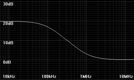
Figure 2: Bode plot showing a typical pole and zero associated with adding CF to the feedback loop. |
 |
 |
Lowpass Budget
There is a risk of overattenuating the highest audio frequencies if the accumulation of lowpass poles is not accounted for. The following formula1 relates the ratio of the lowpass cutoff for n individual stages to the overall system lowpass cutoff.
|
|
For n lowpass poles
| (7) |
fstage = |
fsystem
α |
To manage a highpass budget for n highpass poles:
| (8) |
fstage = |
α × fsystem |
If you are curious as I how the formula for α was derived, begin by equating the value for -3dB to the magnitude function for n identical lowpass poles normalized to a stage lowpass pole of 1 and system lowpass pole of α. Then solve the equation for α:
| (9) | 1 |
1 |
|||||
|
|
= |
|
|||||
|
|
| (10) |
|
= |
|
| (11) | 2 = (α2 + 1)n |
| (12) |
n
2
|
= |
α2 + 1 |
| (13) | α2 = |
n
2
|
-
1
|
|
|
Design Sequence
- Choose a system lowpass cutoff frequency. If some system components are out of design control, estimate a higher cutoff frequency to compensate.
- From the chosen system lowpass cutoff frequency and total number of anticipated lowpass poles, calculate the stage lowpass cutoff frequency for each pole.
- Calculate signal slew-rate limitation imposed by chosen stage lowpass cutoff frequency.
- Design the slew-rate limiting circuitry for each stage based on calculated stage lowpass cutoff frequency.
- Choose or design an open-loop amplifier circuit with maximum slew-rate specification sufficiently above that of signal slew rate limitation for desired safety factor.
- Place the slew-limiting circuitry and feedback loops close to the
amplifiers protected.
A Special Case
Limiting slew-rate in current to voltage converters is extremely important in view of their common use as the first analog stage of current output DACs because they can see considerable RF energy if it is not limited. I believe that applying at least one pole of passive lowpass filtering before the first non-linear component to be an important design consideration. That some DAC schematics show an optional shunt capacitor of unspecified value to ground before i/v conversion shows that DAC chip makers believe so too.| Figure
3:
Current
to
voltage
converter |
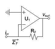 |
The suggested shunt capacitor would create a low impedance lowpass filter with the real input impedance Z'F. To consider this further it is necessary to determine Z'F2, which I expect to present a virtual inductance associated with its dominant pole.
Begin with a textbook specification for Z'F.
| (14) |
Z'F = |
RF + RO
1 + AV-OL |
because of dominant pole at f1:
| (15) |
AV-OL = |
AV-DC
1 + s/2πf1 |
If AV-OL >> 1, then Z'F breaks down to a virtual series inductance and resistance:
| (16) |
Z'F ≈ | (1 + s/2πf1)(RF
+ RO)
AV-DC |
= sL'F-SERIES +
R'F-SERIES |
The inductive part depends on the gain bandwidth of the open loop amplifier:
| (17) |
L'F-SERIES = | RF + RO
2πf1AV-DC |
= |
RF + RO
2π(GBW) |
The resistive part
| (18) |
R'F-SERIES = |
RF + RO
AV-DC |
The one that was dropped between equations (15) and (16) amounts to a resistance in a parallel relationship with the series components:
| (19) |
R'F-PARALLEL = |
RF + RO |
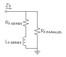
Now we can represent the complex input impedance in the following equivalent circuit:
| Figure
4:
Z'F equivalent circuit |
 |
I did a SPICE simulation with just a shunt capacitor from the inverting input to ground calculated against the virtual inductance to give a cutoff of 100kHz. The sharp resonance peak meant the capacitor shown in this position in DAC datasheets was a hint and not a final solution. Adding CF in parallel with RF to get another pole of filtering as in figure 5 will complicate the input impedance even further. Either way, designing a filter against open-loop specifications that may vary greatly would not be practical.
| Figure 5: Circuit illustrating slew rate limited i/v converter |
 |
If an additional resistor R1 is added to the circuit, a simpler design method can be applied.
- Allot two stage poles to the i/v converter in the lowpass budget.
- Calculate R1 to form a pole with the virtual input inductance high enough above the chosen stage pole frequency to prevent a complex pole in the final circuit, much greater than the i/v converter input resistance R'F-SERIES, and much lower that the equivalent output resistance of the driving current source.
- Calculate C1 with respect to R1 and CF with respect to RF to give the desired stage pole frequencies.
- Choose R1 and C1 parts as linear as possible given goal of reducing RF before nonlinear components in signal path.
|
|
Example
Designing the analog circuit of a DAC/Preamplifier combo would demonstrate most of the principles of this article. The DAC output is presumed source 6.2mA ± 3.9mA. Although this is the output specification of the PCM1792 and PCM1794, no particular DAC is specified because the only the analog design is undertaken. AD826 op-amps were chosen for high-slew rate and the promise of euphony due to their 10kHz dominant pole. For simplicity, the design uses only one of the DAC's differential outputs. Otherwise two extra op-amps would be required.| Figure
6:
Example
schematic
of
the
analog
circuit
of
a
DAC/Preamplifier
|
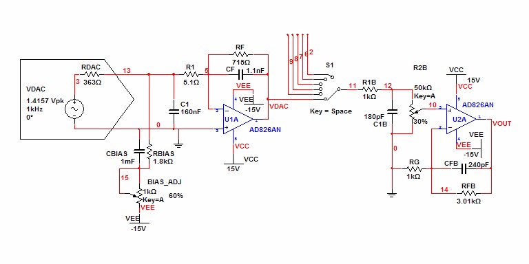 |
| Note: Internal DAC
output model is a reasonable guess. RDAC is not
specified in the
datasheet |
Allot three lowpass poles to the lowpass budget, two for the i/v converter and one for the output buffer.
Although a full system bandwidth of 50kHz would be acceptable, this is not quite a full system. Choose 100kHz for the system bandwidth and calculate the stage bandwidth for 3 system lowpass poles:
|
|
|
| fstage = |
fsystem
α |
= | 100kHz
0.509825 |
= 196.146kHz |
I/V Stage
Because two stage lowpass poles are allotted here, calculate break frequency for entire stage:
|
|
|
| fi/v-stage = |
fstage × α |
= | 196.146kHz × 0.643594 | = 126.238kHz |
Calculate expected signal slew-rate based on chosen stage lowpass pole and 2.82843V peak output signal (2Vrms).
slew-rate = 2πfvpk = 2π × 126.238kHz × 2.82843V = 2.24344V/µs
AD826 minimum slew rate of 300V/µs gives a slew-rate safety factor of:
| safety factor = |
300V/µs
2.24344V/µs |
= 133.723 |
Calculate RF from 7.8mAp-p current input to give 2Vrms output:
| RF = |
2Vrms × 2.82843p-p/rms
7.8mAp-p |
= 725.238Ω |
RF = 715Ω
Calculate virtual inductance at feedback terminal:
| L'F-SERIES = | RF + RO
2π(GBW) |
= |
715Ω + 8Ω
2π(50MHz) |
= 2.30138µH |
Calculate R1 for pole with virtual inductance above system lowpass pole:
| R1 = 2πfL'F-SERIES = 2π × 200kHz × 2.30138µH = 2.892Ω |
Calculate C1 for desired stage lowpass pole:
| C1 = |
1
2πfstageR1 |
= |
1
2π × 196.146kHz × 5.1Ω |
= 159.1nF |
C1 = 160nF
Gain-Buffer Stage
Calculate expected signal slew-rate based on chosen stage lowpass pole and 15V peak output signal.
slew-rate = 2πfvpk = 2π × 196.146kHz × 15V = 18.4863V/µs
AD826 minimum slew rate of 300V/µs gives a slew-rate safety factor of:
| safety factor = |
300V/µs
18.4863V/µs |
= 16.2282 |
The operational amplifier voltage noise specification of 15nV/√Hz calculates to an equivalent noise resistance of 13.5806kΩ. (See article Simple Noise Calculations)
Initially setting RG = 1kΩ would make the resistor contribution to the noise negligible compared to that of the op amp itself.
For a gain of 4 chosen to lower the noise contribution of a desirable op-amp without low noise:
RFB = RG(AV-1) = 1kΩ(4-1) = 3kΩ
Round to nearest 1% value:
RFB = 3.01kΩ
Calculate CFB for desired stage lowpass pole:
| CFB = |
1
2πfstageRFB |
= |
1
2π × 196.146kHz × 3.01kΩ |
= 269.572pF |
CFB = 240pF
This choice of RFB and CFB determine a zero:
| TZ = | TP
AV |
= | RFBCFB
4 |
= | 3.01kΩ × 240pF
4 |
= 180.6ns |
Calculate a pole to match the zero to continue the rolloff of the desired stage lowpass pole
Choose R1B = 1kΩ and potentiometer R2B = 50kΩ, and calculate parallel equivalent:
| RPAR = |
1kΩ × 50kΩ
1kΩ + 50kΩ |
= 980.392Ω |
Calculate C1 from RPAR and the desired pole time constant:
| C1B = |
TZ
RPAR |
= | 180.6ns
980.392Ω |
= 184.212pF |
C1B = 180pF
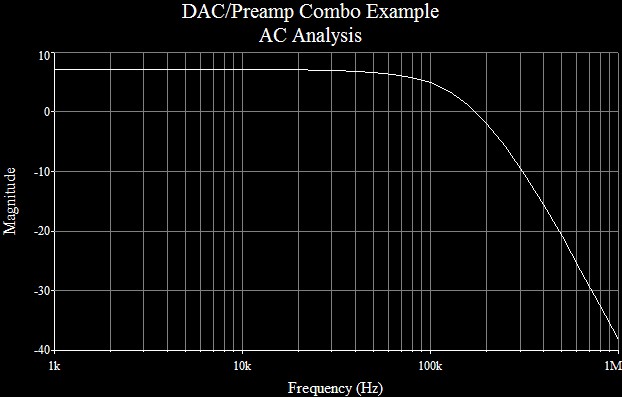
SPICE Results
SPICE does provide a built-in TIM test, so only the lowpass budget results can be verified by the design specifications. Figure 7 below shows a -3dB cutoff slightly higher than the 100kHz set for the system bandwidth. This is the expected result of rounding component values to standard values with a mind to prefer higher frequency poles.
SPICE model for example circuit modeled on Analog Devices edition of Multisim. Right-click and choose Save Link As to obtain file.
| Figure
7:
Lowpass
budget
close
to
chosen
100kHz,
down
only
0.08db
at
20kHz |
 |
|
|
Other Thoughts
Although it is outside the scope of this article, designing the amplifier and its feedback circuit for critical damping (i.e. Bessel response) to minimize ringing may benefit these ends as well.Non-feedback circuits may also benefit from these techniques because of the possibility that signal connections may pick up stray outside signals such as RF which produce undesirable intermodulation with the intended music signal.
|
|
1Ron Mancini, Op Amps for
Everyone, 2001, www.ti.com, p. 16-3.
2The (') mark is used here to indicate
virtual variables to distinguish them from literal ones.
Document History
February 26, 2011 Created.
February 27, 2011 Corrected some misspellings and made few minor
improvements.
April 11, 2011 Made grammar corrections.