 |
| Home │ Audio
Home Page |
Copyright © 2016 by Wayne Stegall
Created January 16, 2016. See Document History at end for
details.
Dual-slope Integrator
Reduce
high
frequency
amplifier
distortion
Introduction
Amplifiers are often diminished in their distortion performance at high frequencies by open loop responses that fall with the slope of a single slope integrator. This occurs whether imposed by the integrator at the front of a delta-sigma class D amplifier or by dominant-pole compensation of a more conventional class A or B types. However, if the integrator slope would fall off at a faster rate, it would impose less reduction in gain as the feedback crossover point is reached. Then lower distortion would prevail to higher frequencies in the closed loop circuit until the approach of the feedback crossover frequency required the loop gain to fall back to unity. The black line in figure 1 below shows a response that suits this task. A second-order slope prevails at lower frequencies until a lowpass zero restores a first-order slope for higher frequencies. This may seem counter intuitive because you would think 180° phase shift at the lower frequencies would create oscillations. However, if the closed loop creates a feedback crossover frequency higher than the zero frequency the global feedback loop will override any such tendency.| Figure
1:
Dual-slope
integrator
response
superimposed
on
related
single-slope
integrator
response. |
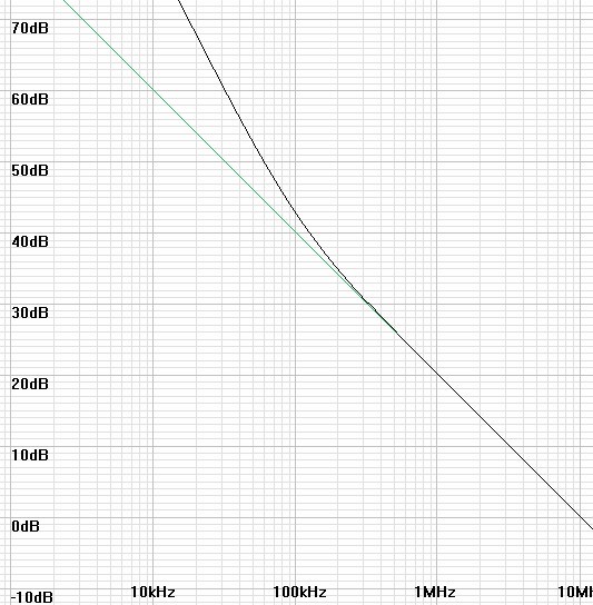 |
| Legend: green: first order integration. black: dual-slope integration. |
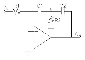
Circuit and Calculations
To get a basis to use this integrator it is necessary to calculate an
analysis of the circuit. The op-amp circuit of figure 2 below was chosen for
simplicity. Although this circuit could appear at the front of a
delta-sigma amplifier, the discrete transistor stage in a class A or B
amplifier would calculate similarly.| Figure
2:
Dual-slope
integrator
implemented
with
operational
amplifier. |
 |
| (1) |
va
vin |
= – | 1
sR1C1 |
, iC1 = |
vin
R1 |
| (2) |
iC2 = iC1 – | va
R2 |
= |
vin
R1 |
+ |
vin
sR1R2C1 |
| (3) |
iC2 = | vin(sR2C1
+ 1)
sR1R2C1 |
| (4) |
vout = va – | iC2
sC2 |
| (5) |
vout = – | vin
sR1C1 |
– | vin(sR2C1+1)
s2R1R2C1C2 |
| (6) |
vout = – | vin(s(R2C2
+R2C1)+1)
s2R1R2C1C2 |
| (7) |
H(s) = |
vout
vin |
= – | sR2(C1+C2)+1
s2R1R2C1C2 |
| (8) |
fzero = |
1
2πR2(C1+C2) |
Above fzero:
| (9) |
H(s) = – | C1+C2
sR1C1C2 |
= |
1
sR1(C1 <series> C2) |
|
|
Closed Loop
Now lets close the global feedback loop as in figure 3 below and analyze again.| Figure
3:
Dual-slope
integrator placed into context with additional open-loop gain and the
application of global feedback. |
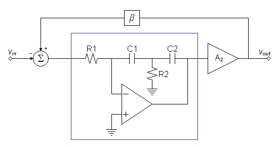 |
Text
| (10) |
H(s) = |
A
1+Aβ |
| (11) |
H(s) = |
|


| (12) |
H(s) = | sA2R2(C1+C2)
+
A2
s2R1R2C1C2 + sβA2R2(C1+C2) + βA2 |
| (13) |
H(s) = | sR2(C1+C2)
+
1
|
| In the form |
s2 ω02 |
+ |
s
ω0Q |
+ 1 |
| (14) |
ω0 = |
|
| (15) |
Q = |
R2(C1+C2) |
= |
1
C1+C2 |
|
| (16) |
Q = | ωzero
ωpole |
Application
Although full calculations have been made, real applications would fall into a more complex stability analysis with other poles adding phase shift. So its seems that equations 8 and 9 become most useful: equation 9 to place the first-order integration in its proper place then equation 8 to set the zero below the feedback crossover frequency by an amount deemed proper for the overall effect in the SPICE analysis and the hardware prototype.SPICE Verification
For SPICE verification the feedback summing node of figure 3 was moved to the inverting terminal of the integrator's op amp. The result is shown in figure 4 below.| Figure
4:
Circuit
used
for
SPICE
verification
|
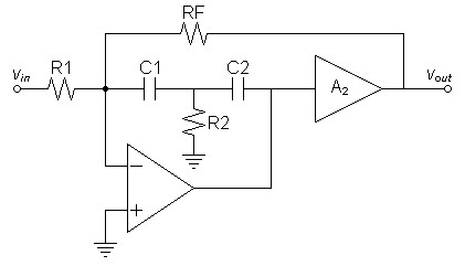 |
The SPICE amplifier simulated is specified for:
- Global feedback to get 30dB passband gain
- A2 = 100 or 40dB
- Integrator based on ideal op amp of 100dB gain.
- 100kHz feedback crossover frequency.
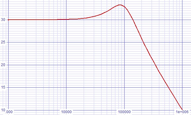
The first simulations puts fzero at the feedback crossover frequency to see how bad the peak is there.
| Figure 5: SPICE deck configured for fzero = ffeedback-crossover. |
| * dual slope
integrator example * Spice Opus 2.31 v1 vin 0 dc 0 ac 1 sin 0 0.1V 1kHz r1 vin vn 1.62k c1 vn vc1c2 6.19n r2 vc1c2 0 130 c2 vint vc1c2 6.19n eopa vint 0 0 vn 100k ea2 vout 0 vint 0 100 rf vout vn 51.1k .end .control set units=degrees ac dec 20 1k 1meg plot db(vout) .endc |
| Figure 6: ≈ 3.5dB peak configured for fzero = ffeedback-crossover. |
 |
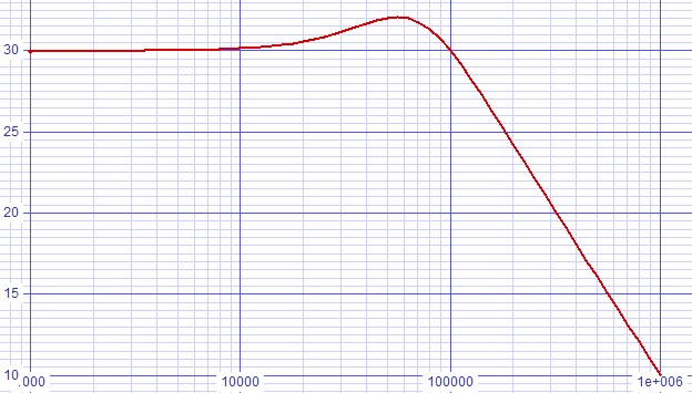
The second simulations puts fzero at the half of the feedback crossover frequency to see how much the peak is reduced.
| Figure 7: SPICE deck configured for fzero = ½ffeedback-crossover. |
| * dual slope
integrator example * Spice Opus 2.31 v1 vin 0 dc 0 ac 1 sin 0 0.1V 1kHz r1 vin vn 1.62k c1 vn vc1c2 6.19n r2 vc1c2 0 255 c2 vint vc1c2 6.19n eopa vint 0 0 vn 100k ea2 vout 0 vint 0 100 rf vout vn 51.1k .end .control set units=degrees ac dec 20 1k 1meg plot db(vout) .endc |
| Figure 8: ≈ 2dB peak configured for fzero = ½ffeedback-crossover. |
 |
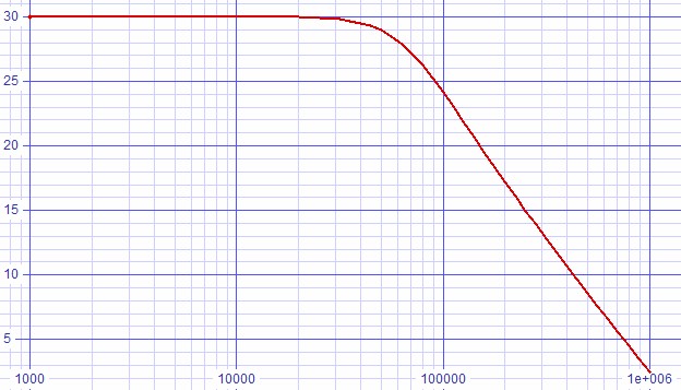
Additional experimentation reveal some additional lowering of peak at the cost of a much lower zero frequency. This is undesirable because much of the gain in lower distortion is lost as the the zero frequency is lowered. It is perhaps desirable to accept the ≈ +0.5dB rise at 20kHz for a distortion improvement. At this point, I did additional experimentation with adding lead compensation to the global feedback loop: i.e. feedback capacitance CF in parallel with the RF already specified. Setting fzero back to the feedback crossover frequency produced excellent results with an experimentally chosen value of lead compensation.
|
|
| Figure 9: SPICE deck configured back to fzero = ffeedback-crossover with lead compensation added at an experimentally chosen value. |
| * dual slope
integrator example * Spice Opus 2.31 v1 vin 0 dc 0 ac 1 sin 0 0.1V 1kHz r1 vin vn 1.62k c1 vn vc1c2 6.19n r2 vc1c2 0 130 c2 vint vc1c2 6.19n eopa vint 0 0 vn 100k ea2 vout 0 vint 0 100 rf vout vn 51.1k cf vout vn 43p .end .control set units=degrees ac dec 20 1k 1meg plot db(vout) .endc |
| Figure 10: No peak when configured back to fzero = ffeedback-crossover with lead compensation added at an experimentally chosen value. |
 |
|
|
Document History
January 16, 2016 Created.