 |
| Home │ Audio
Home Page |
Copyright © 2015 by Wayne Stegall
Created March 5, 2015. See Document History at end for details.
| > |
Distortion Grapher
Circuit
enables
distortion
error
to be graphed
Introduction
In other articles, SPICE analysis was used to analyze the shape the distortion error of various amplifiers and circuits. Here I want to suggest a circuit to allow the same analysis to be done to live circuits. The idea is to drive the circuit with a signal generator, attenuate the output of the circuit back to the input level, then subtract the result from the same input signal to return the distortion error curve. The signal would then be graphed on an oscilloscope.In mathematical terms if a circuit can be defined as having gain (AV) + error (ε) and ε is scaled as if introduced before the gain.
| (1) |
Vout = AV(Vin + ε) |
Solving for error gives the equation of a device that will show that error.
| (2) |
ε | = |
Vout
AV |
– | Vin |
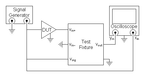
The diagram in figure 1 below shows how such a device would be connected to allow the graphing of the distortion error.
| Figure
1:
Connection
of test fixture with other components to graph
distortion error. |
 |
Circuit Design
Of the possible topologies that in figure
2 uses the least number of operational amplifiers.| Figure
2:
Schematic
of Distortion grapher test fixture. |
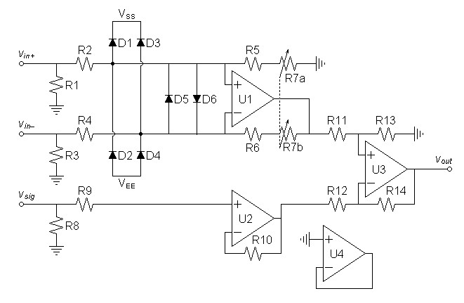 |
Choose operational amplifier. It is desired that the operational amplifier have noise and distortion well below the distortion levels to be graphed. Then it is desired the operational amplifier be a type that has no design peculiarities that might produce unexpected results. My first thought to use the AD797 fits the first qualification but not the second. The OPA227 fits the second specification with only a slightly higher noise level. Use the 4 circuit version: OPA4227. If the AD797 is desired the circuit may have to be modified.
Want R3 and R4 to dissipate only ½ Watt when driven at a voltage giving 1000W into 8Ω.
| (3) |
R3 = |
8Ω × 1000W
½W |
= 16kΩ |
Define R5 and R6 to define some maximum attenuation for a worst case where 1000W is produced from a 250mV input.
| (4) |
V@1000W = |
2PR |
= |
2 × 1000W × 8Ω | = 126.491V |
| (5) |
R5 = |
20kΩ × 250mV/126.491V | = 39.5285Ω |
R5 and R6 might be omitted without problems.
Choose 1kΩ for R11 and R12 then calculate R13 and R14 for a voltage gain of 10.
| (6) |
R13 = 1kΩ × 10 = 10kΩ |
Other components are chosen arbitrarily according to familiar practice. Also for now, it is presumed that the reader knows how to construct a conventional operational amplifier power supply of ±15V.
| Figure 3: Parts List |
||||||
| U1-U4 |
OPA4227 |
R7 |
20kΩ dual potentiometer, ½W | |||
| D1-D6 |
1N914 or 1N4148 | R9, R10 |
100Ω | |||
| R1, R3, R8 | 47kΩ | R11, R12 |
1kΩ | |||
| R2, R4 | 20kΩ, 1%, 1W | R13, R14 |
10kΩ | |||
| R5, R6 |
39.2Ω | |||||
Optionally small capacitors might be placed in parallel with R1, R3, and R8 if you desire some rf filtering on the inputs.
Operation
- Refer to figure 1.
- Set text figure potentiometer R7 to maximum attenuation.
- Connect signal generator to input of device under test (DUT) and to its input to test fixture. Connect DUT to test fixture: Non-inverting single ended circuits to vin+, inverting single ended circuits to vin–, or bridged outputs to vin+ and vin–.
- Connect output of text fixture to y input and signal generator to x input of oscilloscope.
- Connect all grounds in common.
- Set oscilloscope to x-y graph mode and make any initial and continuing adjustments necessary to properly scale the graph.
- Adjust sine or triangle wave amplitude of signal generator for
desired output from DUT.
- Raise R7 until outputs of DUT and signal generator appear to cancel.
- Increase y-signal gain of oscilloscope to show full-screen
display of distortion error and adjust R7 again if needed
for better cancellation of the test signal.
|
|
Document History
March 5, 2015 Created.