 |
| Home │ Audio
Home Page |
Copyright © 2011 by Wayne Stegall
Updated June 14, 2011. See Document History at end for
details.
Partially SPICE Verified
Distortion Cancelation
Introduction
It is the purpose of this article to introduce simple distortion cancelation concepts. All function to linearize one device with another device having the same transfer equation perhaps scaled in some applications. The transfer functions are represented in this article as follows:Transconductance transfer function
| (1) |
i = g(v) |
Transimpedance transfer function
| (2) |
v = g-1(i) |
In this designation the suffix -1 indicates an exact inverse equation so that:
| (3) |
g-1(g(x)) = g(g-1(x)) = x |
This relation relates the mathematical operation of the first two distortion cancelation techniques.
Current Mirror
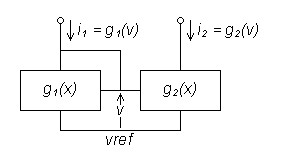
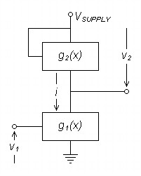
| Figure 1:
Generalized Current Mirror |
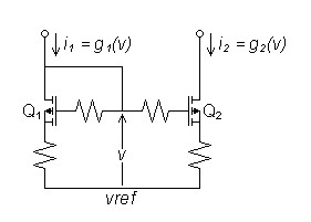
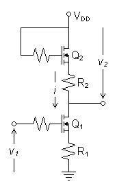
Figure 2:
MOSFET Current Mirror |
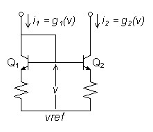
Figure 3:
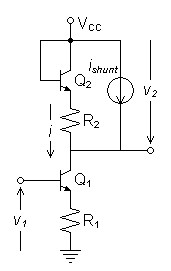
BJT Current Mirror |
 |
 |
 |
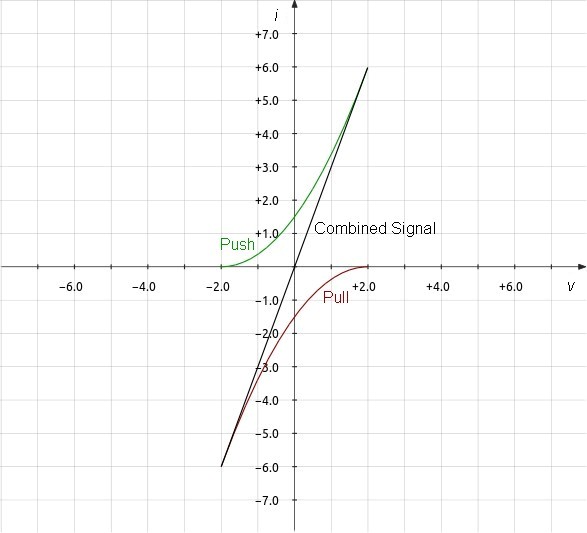
| Figure 4: Graph
Illustrating Current Mirror Operation |
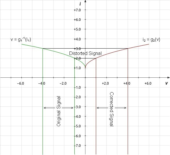 |
A current mirror duplicates its input current in the output by means which cancel distortion. The input transistor or amplification block converts current to voltage by the inverse of the transfer function g1(x) by which the second amplification block converts voltage to current:
Transimpedance creates distortion.
| (4) |
v = g1-1(i1) |
Distortion cancelation removes it.
| (5) |
i2 = g2(v) |
Because g1(x) = g2(x):
| (6) |
i2 = g2(g1-1(i1)) = g1(g1-1(i1)) = i1 |
Transistors and feedback resistors must be in matched pairs. Because the feedback resistors are present to reduce any semiconductor mismatches, they are often omitted when the matched transistors are created equally on the same silicon die. I.e. in an IC or a dual transistor device.
If you can pair devices so that the transfer curves match on a scale, current amplification is possible.
Assuming g2(x) = ACURR × g1(x):
| (6) |
i2 = g2(g1-1(i1)) = ACURR × g1(g1-1(i1)) = ACURR × i1 |
This attempt to add gain may shift the voltage bias so that the transconductance blocks may require termination by different reference voltages to restore proper distortion cancelation, however.
Equations adding gain to the current mirror above and the voltage mirror below extrapolate from presumptions based on linear devices. Actual results may vary and calculations based on device parameters will depend on the extent to which the non-linear transfer curve has scale symmetry and will differ according to the device used.
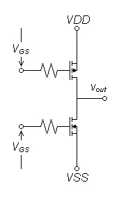
Voltage Mirror
| Figure 5:
Generalized Voltage Mirror |
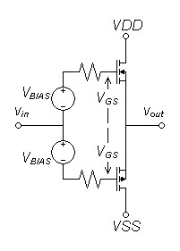
Figure 6:
MOSFET Voltage Mirror |
Figure 7:
BJT Voltage Mirror |
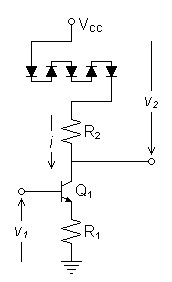
Figure 8: Integer Gain BJT Voltage Mirror |
 |
 |
 |
 |
| Figure 9: Graph
Illustrating Voltage Mirror Operation |
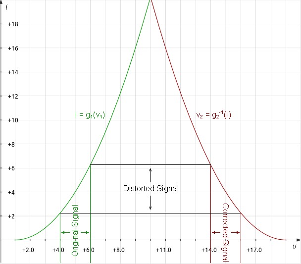 |
The voltage mirror duplicates the input voltage at the output by means which cancel distortion. The amplifying block converts voltage to current by the same transfer function g1(x) as the distortion cancelation device uses to cancel distortion, designated g2(x) to allow scaling.
Transconductance creates distortion.
| (7) |
i = g1(v1) |
Distortion cancelation removes it.
| (8) | v2 = g2-1(i) |
Because g1(x) = g2(x):
| (9) |
v2 = g2-1(g1(v1)) = g1-1(g1(v1)) = v1 |
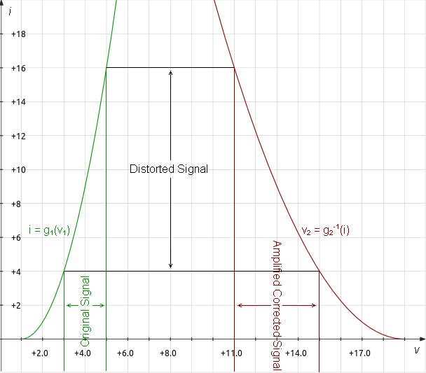
Because distortion here is cancelled in a common-source or common-emitter circuit where gain is expected, the cancelation factors must be scaled. Assuming g1(x) = AV × g2(x), therefore g2-1(x) = g1-1(AV × x) and:2
| (10) |
v2 = g2-1(g1(v1)) = g1-1(AV × g1(v1)) = AV × v1 |
| Figure 10: Graph
Illustrating Amplified Voltage Mirror Operation |
 |
FET specifics
Because the resistors must be scaled inversely to the transconductance parameters, the following relations hold:1
| (11) |
gfs1 = AV × gfs2 |
| (12) |
R2 = AV × R1 |
| (13) |
gfs1 × R1 = gfs2 × R2 |
Because the mirror is connected by the common drain current and
| (14) |
gfs = 2 x | knID |
Relations involving kn can be established
| (15) |
kn1 = AV2 × kn2 |
| (16) |
kn1 × R12 = kn2 × R22 |
BJT specifics
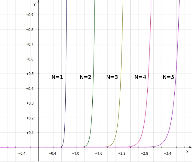
The exponential transfer function of the BJT permits distortion cancelation. This is because the exponential function involved has a unique symmetry where scaling the current appears to shift the same curve to a different voltage bias.
The base-to-emitter PN junction (diode) that creates this unique symmetry has the function and is illustrated in figure 11 below for N=1:
| (17) |
ipn = i0(ev/VT-1) |
Because the resistors must be scaled inversely to the transconductance parameters, the following relations hold for gain AV:
| (18) |
gm1 = AV × gm2 |
| (19) |
R2 = AV × R1 |
| (20) |
gm1 × R1 = gm2 × R2 |
Where the characteristic PN voltage VT ≈ 25mV, transconductance is proportional to current:
| (21) |
gm = |
IE
VT |
≈ | IE
25mV |
This works well enough if the gain is one.
Topology Compensating in Gain with One Compensation Device (Not recommended).
Thus to lower gm2 relative to gm1 to set cancelation with gain in one device, it is necessary to lower the current bias through Q2. Figure 7 shows the use of a DC current shunt around the cancelation circuit to accomplish this objective. That the DC bias voltage across R1 and R2 are equal as a result of this adjustment if the transistors are matched is a convenient coincidence.
Because gm is tied to bias current for any PN junction according to equation (21), no one device can compensate for a BJT in a gain situation without current bias change.
I believe now that this method destroys symmetry and the resulting distortion reduction is done at the sacrifice of creating two bends in the transfer curve. Without symmetry, it is not strictly a voltage mirror. Use the following topology instead. I intend to delete this topology from the article once I am sure of this outcome.
Integer Gain BJT Voltage Mirror Topology (Preferred Topology)
For integer gain of N, a direct solution is to use N compensation devices in the load as in figure 8. The combined transconductance for N series compensation devices is:
| (22) |
gm2 = |
IC
N × VT |
≈ | IC
N × 25mV |
If gm1 is calculated by equation (21) and gm2 by equation (22) and , equations (18)-(20) relate the design equations for gain. This would have been the first topology to try had it not been for my bias against using so many diodes or transistors in the compensation circuit. However, this bias may not have any validity as the shared current forces all of the diodes to respond as one. There are practical limits to N however; consider that ten diodes will drop about 7V.
| Figure
11:
I/V
Curve
of
Series
Diodes
Scale with Symmetry with Increase
in N. |
 |
Square Law cancelation
| Figure
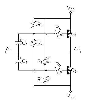
12: MOSFET Push-pull Common Source Amplifier |
Figure
13: MOSFET Push-pull Voltage Follower |
 |
 |
| Figure 14: Graph
Illustrating Square Law Distortion Cancelation |
 |
That FETs and vacuum tubes have square-law transfer curves enable a common distortion cancelation technique. Arrange two square law devices so that their linear signal components add while their second-order components subtract.
In the case of opposing n-ch and p-ch FETs:1
| (23) |
IDn = kn(VGSn - VTn)2 |
| (24) |
IDp = kp(VGSp + VTp)2 |
If they are connected to oppose one another:
| (25) |
IOUT = kn(VGS - VTn)2 - kp(VGS + VTp)2 |
| (26) | IOUT = kn(VGS2 - 2VGSVTn + VTn2) - kp(VGS2 + 2VGSVTp + VTp2) |
| (27) | IOUT = (kn(-2VGSVTn) - kp(2VGSVTp)) + (kn(VGS2 + VTn2) - kp(VGS2 + VTp2)) |
| (28) | IOUT = (kn + kp)(-2VGS)(VTn + VTp) + (kn - kp)VGS2 + (knVTn2 - kpVTp2) |
If kn = kp then second order term cancels leaving:
| (29) |
IOUT = (kn + kp)(-2VGS)(VTn + VTp) |
The term (knVTn2 - kpVTp2) is constant and infers biasing which was omitted for simplicity.
If cancelation is imperfect the result will be as if the circuit were single-ended, the transfer curve bent in the direction of the greater of kn or kp. Adding source resistors in this application will increase distortion by altering the square-law transfer characteristic. They should only be added to correct imbalances between device source or cathode ohmic resistances if necessary.
Any difficulty in matching devices could be overcome by using dual FET arrays of the same polarity packaged in a single semiconductor. This would require transformer coupling on both the input and output to correctly juxtapose the device characteristics to produce this result, a typically tube topology.
SPICE Results
Current MirrorCurrent mirrors are well established enough in principle for unity gain versions not to need SPICE verification yet.
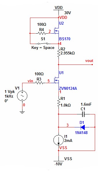
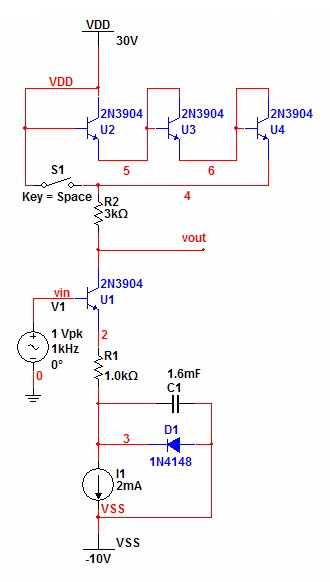
| Voltage Mirror | Figure
15:
SPICE
Example:
Amplified
MOSFET
Voltage
Mirror |
||||||||||||||||
| A preliminary SPICE evaluation
of a unity gain MOSFET voltage mirror
gave near perfect results. Calculate distortion correction for
SPICE
simulation of amplified MOSFET voltage mirror: Given kn1 of ZVN0124A = 1.077A/V2 kn2 of BS170 = 123.3mA/V2 and R1 = 1kΩ Calculate R2 for distortion cancellation and arbitrary gain from equation (16) above:
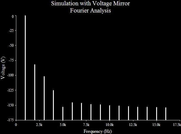
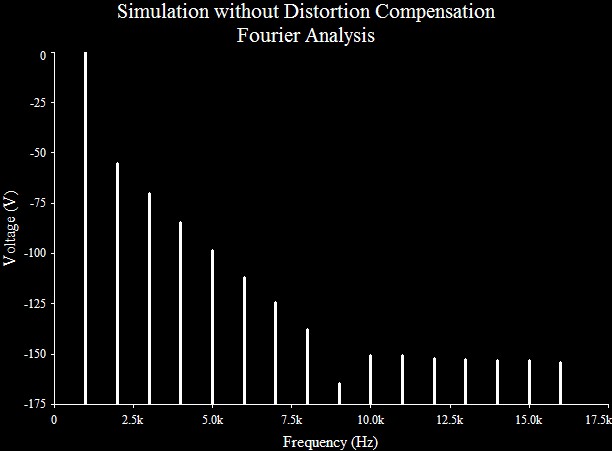
SPICE Model - Amplified Voltage Mirror (Multisim Analog Devices Version 10.0.1). For the simulation, switch S1 is provided to compare the results. If S1 is open the circuit operates with distortion cancelation. As such the distortion result was 0.0000465395%. Closing S1 bypasses the distortion cancelation. This result was 0.100808%. The graphs below show the details. The preliminary simulation without gain produced similar results. SPICE Model - Unity Gain Voltage Mirror (Multisim Analog Devices Version 10.0.1). If you are curious, the subcircuit consisting of I1, C1, and D1 represent an idealized autobias circuit. C1 holds the voltage bias that would be required for AC fluctuation about a DC bias current of I1. Calculate the highpass pole R1C1 for a low frequency minimizing any affect on bass response.
C1 = 1.6mF (In practice, I should have chosen a 20% value of 2.2mF) |
 |
| Figure
16:
MOSFET
Voltage
Mirror
Distortion
Profile.
Switch
S1
open |
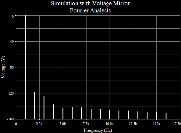 |
Figure 17: MOSFET Distortion profile with Compensation Bypassed. Switch S1 closed. |
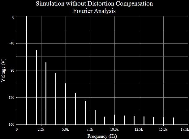 |
| BJT Voltage Mirror | Figure 18: SPICE Example: Integer Gain BJT Voltage Mirror | ||||
| SPICE verified excellent results
with the BJT voltage mirror only for
unity gain. With gain, SPICE showed inconsistent results. I
believe the culprit is the topology that reduces bias to the
load. Decreasing bias by the same ratio by which the signal is
increased is a bad idea. Distortion is inversely proportional to
bias, the reduction in bias possibly eliminating any gains created by
the compensation circuit. Experimentally however, some values of
load current bias produced excellent cancelation results, but not those
calculated. It is possible that distortion cancelation increases
as the load bias current decreases toward the target until proximity to
signal clipping ends any further gains. Initial evaluation of an integer gain BJT voltage mirror produced ambiguous results until I thought the uncompensated circuit had such low distortion that interpolation error in SPICE might obscure any improvement. Only after I reduced the bias until the uncorrected circuit showed modest distortion was I able to demonstrate distortion cancelation. For the SPICE Example: Integer Gain BJT Voltage Mirror of figure 18 distortion cancelation lowered the distortion from 0.176063% to 0.0076505%.
|
 |
Push-pull Common Source Amplifier Model Demonstrating square-law cancelation
| Figure 21: SPICE Example Push-pull Common Source Amplifier |
 |
| This circuit is so simple that you may
have seen it before. |
SPICE Model - Push-pull Common Source Amplifier (Spice Opus version 2.31)
This model is setup for perfect distortion calculation with plausible MOSFET models. Only the third harmonic has any significance at -90dB. Distortion analysis is done at a peak voltage only half that of the supply because the non-feedback circuit exhibits soft-clipping at peak voltages approaching supply voltage.
Fourier analysis for vout:
No. Harmonics: 16, THD: 0.00308134 %, Gridsize: 1024, Interpolation Degree: 3
| Harmonic | Frequency | Magnitude | Norm. Mag | Percent | Decibels |
|
|
|
|
|
|
|
| 1 | 1000 | 11.0989 | 1 | 100 | 0 |
| 2 | 2000 | 1.89998e-08 | 1.71186e-09 | 1.71186e-07 | -175.3306351 |
| 3 | 3000 | 0.000341991 | 0.000030813 | 0.0030813 | -90.22532032 |
| 4 | 4000 | 6.13527e-10 | 5.5278e-11 | 5.5278e-09 | -205.1489536 |
| 5 | 5000 | 1.71547e-06 | 1.54562e-07 | 1.54562e-05 | -136.2179454 |
| 6 | 6000 | 2.87887e-10 | 2.59383e-11 | 2.59383e-09 | -211.7211698 |
| 7 | 7000 | 1.82522e-07 | 1.6445e-08 | 1.6445e-06 | -155.6793224 |
| 8 | 8000 | 2.36409e-10 | 2.13001e-11 | 2.13001e-09 | -213.4323672 |
| 9 | 9000 | 2.05443e-08 | 1.85102e-09 | 1.85102e-07 | -174.6517778 |
| 10 | 10000 | 1.93555e-10 | 1.74391e-11 | 1.74391e-09 | -215.1695186 |
| 11 | 11000 | 2.38049e-09 | 2.14479e-10 | 2.14479e-08 | -193.3723045 |
| 12 | 12000 | 1.63528e-10 | 1.47337e-11 | 1.47337e-09 | -216.6337635 |
| 13 | 13000 | 3.27712e-10 | 2.95265e-11 | 2.95265e-09 | -210.5957606 |
| 14 | 14000 | 1.36697e-10 | 1.23162e-11 | 1.23162e-09 | -218.1904653 |
| 15 | 15000 | 1.27771e-10 | 1.1512e-11 | 1.1512e-09 | -218.7769844 |
|
|
1SPICE MOSFET models represent
both kn and kp as KP. JFET models call this
parameter BETA.
2I am taking some liberties with my math
here because of the expectation of scale symmetry between g1(x)
and
g2(x).
Document History
May 26, 2011 Created.
May 26, 2011 Made minor improvements and corrections as
noticed. Added scematic for SPICE example
push-pull common-source amplifier and changed corresponding spice deck
to match new component labels.
May 27, 2011 Corrected some hasty presumptions pertaining to
adding gain to mirror circuits, particularly equations relating AV
to kn for the MOSFET voltage mirror.
May 27, 2011 Added graphs illustrating distortion cancelation
concepts.
May 31, 2011 Added SPICE verification of MOSFET voltage mirrors.
June 8, 2011 Recommended use of voltage mirror for BJT circuits
only for unity gain pending further investigation. SPICE results
problematic with gain, only unity gain producing the desired
results. See text.
June 11, 2011 Added SPICE verification of integer-gain BJT
voltage mirror.
June 14, 2011 Corrected a spelling mistake.