 |
| Home │ Audio
Home Page |
Copyright © 2013 by Wayne Stegall
Updated January 16, 2013. See Document History at end for
details.
Delta-Sigma Modulators
Their
basic
theory
of
operation
Introduction
It was possible that I created curiosity about delta-sigma modulators in my previous article Digital Audio Formats. To satisfy any such curiosity I describe here their method of operation. It may be useful to reread that article as a prerequisite to this one.Digital Modulator
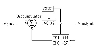
It is useful to begin by explaining a first-order digital delta-sigma
modulator. To produce a bitstream with an average value
proportional to an analog input (or its PCM equivalent), it is
necessary to track and conserve input energy as it is output in
constant
pulses. In the following flowchart, the accumulator tracks this
energy. Input values are added to the accumulator as they are
received, the accumulator acting functionally as a digital
integrator. A positive balance in the accumulator requires a
positive binary output value (1) and a negative balance requires a
negative binary output value (0) for proper representation. Then
a constant value N is subtracted or added respectively to track the
energy deployed to the output to represent the input signal. This
creates a feedback loop that ensures that all of the input energy is
represented at the output with some uncertainty as to which exact
pulses and how many will be involved in the representation. It is
assumed that the output frequency is much greater than the maximum
input signal frequency so that many bits can represent each positive
and negative swing. DSD and many DACs modulate the bitstream at
64x to 128x the normal 2x sampling rate specified as a minimum for
PCM.| Figure
1:
Flowchart
of
digital
modulator |
 |
| Figure
2:
Pseudocode |
|
main()
{ on
arrival of input sample
accumulator = accumulator + input;
on out_clock{ if(accumulator >=0.0)
}output = 1;
elseoutput = 0;
if(output == 1)feedback = N;
elsefeedback = -N;
accumulator = accumulator - feedback;}
|
Noise Shaping
At first glance this algorithm seems to have a fatal flaw. 64 or
128 bits per up or down swing of a signal seems only to be able to
represent the same number of discrete levels of signal. Thus 64x
sequential bits would seem only to have 6 bits of equivalent PCM
resolution and 128x only one bit more. However another factor is
at work so that that much greater resolution is attained. There
is additional room for level coding in the arrangement of any
particular number of ones and zeros. This is because the actual
arrangement of ones and zeros determine a short term frequency spectrum
that, depending on the exact sequence can distribute the represented
energy in many different ratios between the near-audible part of the
spectrum and the inaudible. After lowpass filtering, which even
the human ear will do, only the energy in the near-audible part of the
spectrum will contribute its part to the overall level. This
process falls under the topic of noise-shaping and enables a claim that
a 64x bitstream can represent 20-bits of resolution at an equivalent
PCM rate of 96kHz.Analog Modulators
At this point the process of noise shaping may seem a mystery.
However examination of analog delta-sigma modulators will make the
nature of its operation clear. In figure 3 below, an integrator
composed of the op-amp, R1, and C1 performs the
function of the
accumulator. In particular, capacitor C1 holds and
manages the
input energy until it is spent at the output. The comparator then
performs the decision whether the energy in C1 should
produce at any
time a positive (one) or negative (zero) level on the output. The
clocked D latch or flip-flop ensures that the comparator decision is
held for an entire clock cycle. The feedback resistor RF
then
subtracts the energy of the output pulse from the capacitor to register
the current cycle's progress toward representing the input signal at
the
output. In contrast to the discrete tracking of energy in the
digital modulator, C1 is continuously charged by the input
and output
in feedback system toward the goal of always spending the energy in the
capacitor toward draining it to zero volts. As with the digital
modulator, this process ensures that the digital output bitstream has
an average energy density that correctly represents the analog input
needing only the proper analog filter to restore a scaled replica of
the original input signal.| Figure 3: First-order analog modulator |
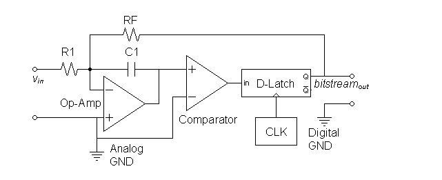 |
| Note: Analog ground here
represents a reference level at the midpoint of digital output range. |
How does this enlighten the process of noise-shaping? Examined simply as an analog system, the modulator has a multiple-feedback arrangement that can be analyzed the same if it were only a simple amplifier. The integrator can be seen viewed as an open-loop block and the application of feedback through RF determines the overall gain. In this context, the operation of the modulator can be understood in terms of the effect of the feedback. Feedback present in the signal band forces compliance of the output to the input for inband frequencies. At some frequency determined by C1, RF, and the apparent gain of the digital block, feedback is released so that digital output swings can occur in out-of-band frequencies. Noise-shaping then is the way that the feedback curve shapes the distribution of the of the out-of-band noise spectrum pertaining to the digital switching activity. The noise spectrum will take the shape of the inverse of the feedback-factor scaled to represent the total out-of-band noise to be represented. In feedback theory terms this is:
| (1) |
E(s) = |
K
1 + Aβ |
In this case A will represent the integrator gain and β will represent the gain setting feedback factor imposed by RF. Thus
| (2) |
E(s) = |
K
1 + (ωint/s)(RF/R1) |
Merging scale factors in the denominator the result is:
| (3) |
E(s) = |
K
1 + ωsystem/s |
After manipulating to a standard form, it is seen that the noise distribution function is a high-pass function complementary to the lowpass function expected to define the in-band response.
| (4) |
E(s) = K |
s
s + ωsystem |
Of course this spectrum is limited on the upper end by the modulation clock frequency.
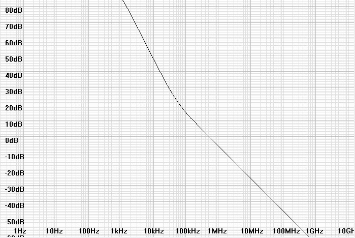
| Figure
4:
Signal
and
modulation
noise
spectrums
of
first
order
modulator.with
signal
to
noise
crossover
frequency
of
100kHz
and
modulation
clock
of
2.8MHz. |
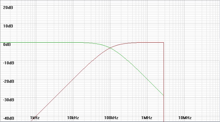 |
| Legend: Green: Signal magnitude response. Red: Modulation noise spectrum. Neither to scale in magnitude. |
Higher-order Modulators
From the bode plot in figure 4 above, it may appear that a first-order modulator may not satisfy high-fidelity audio design requirements. Because the first-order transition from signal band to noise band is slow, feedback that would reduce distortion and quantization noise in the upper audio frequencies is low. Distortion performance is improved by increasing the slope of the transition and therefore the order of the modulator. Digital modulators go as high as the seventh order because digital techniques can achieve high orders with minimal phase shift. Analog techniques generally run into phase shift limitations that limit the slope of the transition. The second-order modulator of figure 5 below is as advanced as reasonable without using some more exotic technology.| Figure
5:
Second-order
analog
modulator |
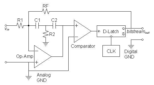 |
| Note: Analog ground here represents a reference level at the midpoint of digital output range. |
The design of the second order modulator is complicated by excessive phase shift in the second-order integrator. Figure 6 below shows that the integrator has a second-order slope slope up to a frequency where a zero restores a single order slope. Because phase shift in the double slope section can approach 180º compared to 90º for the single slope section, the integrator can be unstable unless the global feedback is greater than the integrator feedback at those frequencies. Therefore the release of feedback to allow the transition from the signal band to the noise band must occur above the zero frequency, shown in figure 6 as 50kHz. If this transition frequency is not high enough above the zero a undesirable resonant peak will occur. The lower the frequency at which the transition occurs the higher the system Q will be and the higher the transition frequency the lower the final system Q. If set up properly, the double slope in the signal band will greatly increase the feedback resulting in lower distortion.
| Figure
6:
Bode
plot
of
representative
second-order
integrator
response |
 |
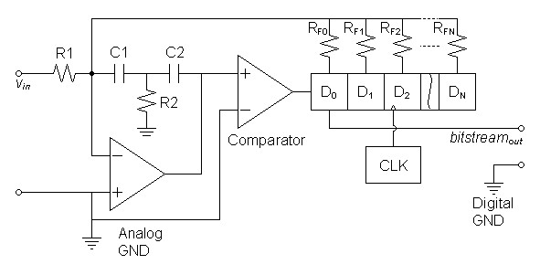
The modulator in figure 7 below seems to take the analog modulator as far as it will go. Instead of taking feedback from the output of one D-type flip-flop this circuit puts an analog FIR filter in the feedback path. The shift-register of D0-DN creates the series of past signal samples ordinarily needed for a digital filter and the corresponding resistors sum to create the filter function. Because a FIR filter can create a sharp cutoff with little or no phase shift, the gain of the integrator can be raised to give much greater distortion suppression than the simpler analog methods above. Because unnecessary delay is undesirable in a feedback loop the filter type would have to associate the greatest filter weight to the tap off of the first flip-flop D0. If this were a brickwall filter it would have to be the apodizing type to prevent unnecessary loop delay. Analog FIR filters of this type make excellent DSD filters and are used in many DACs like the PCM1794 to filter DSD streams. Functionally, as lowpass filters, they change the DSD stream containing the embedded analog signal to a PAM signal at the same clock frequency more closely resembling the analog result with no additional magnitude quantization.
| Figure
7:
High-order
analog
modulator |
 |
Notes:
|
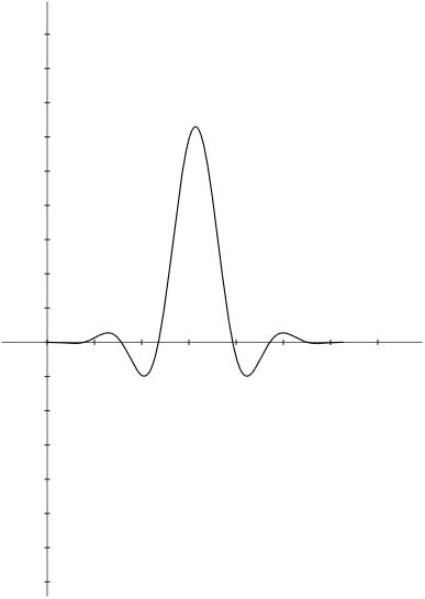
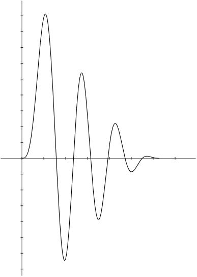
| Figures 8 and
9: Illustration of delay issues in the design of the analog FIR
filter used in the modulator of figure 7 above. |
|
| a –
Brickwall filter delays
signal by half of kernel time. |
b –
Apodizing filter moves
center of kernel more toward the beginning. |
 |
 |
Applications
- ADC front ends
- DAC back ends
- DSD creation
- Class-D amplifiers
|
|
Document History
January 15, 2013 Created.
January 16, 2013 Corrected some grammar and added an extra phrase
of
text and graphs of analog FIR filter kernels.