 |
| Home │ Audio
Home Page |
Copyright © 2012, 2013 by Wayne Stegall
Updated January 2, 2013. See Document History at end for
details.
DAC Cascode
Introduction
Current to voltage conversion is commonly needed to convert the output of many DACs. For any who requires a single transistor converter rather than the usual op-amp I/V converter, the BJT cascode is most obvious candidate.PNP Circuit
| Figure 1: Schematic of
single-ended analog circuit.. |
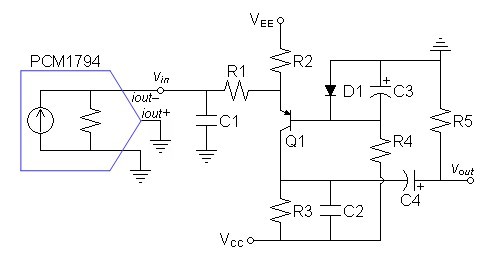 |
| Note: Only left channel
shown. Duplicate for the right channel. |
The circuit of figure 1 above adds several features to the ordinary BJT cascode of Q1. R2 increases the bias through Q1 to lower overall distortion. D1 biases the emitter of Q1 to ≈ 0V. C3 removes nonlinearities from drive to Q1 base for the calculated range of higher frequencies and prevent RF from intermodulating in D1. C1 and C2 create two synchronous lowpass poles with respect to their related resistances to give an overall cutoff frequency of 100kHz. C1 in particular is positioned before Q1 to reduce intermodulation with DAC RF frequencies. R1 is added to reduce variations in AC emitter impedance related to signal level which tend to create a changing pole frequency with respect to C1. As for the unused diffential DAC output, it is reasonable to connect it separately to the same voltage that the other sinks into.
This design for the PCM1794 will also work for the comparable PCM1792 also. For other current output DACs as the other PCM179x (the PCM1795, PCM1796, and PCM 1798), it would be necessary to recalculate for the different current output specifications. If the DAC sinks current rather than sources it as these do, the circuit polarity could be flipped and an NPN transistor used instead of a PNP. The AD1955 is one of these, not only requiring a NPN design but slightly different biasing as well.
First Try with PCM1794
I set R3 and R5 to the same value in the first
attempt thinking R3 could drive an equal resistance in R5
with R5 perhaps off the circuit board at the output
jack. Placing R5 at the end of dedicated interconnects
could even eliminate cable effects.Evaluate Datasheet
The datasheet for the PCM1794 gives the following output specifications:| AC output |
|
7.8mA peak-to-peak for each
single-ended output (I use the 3.9mA peak value in the calculations) |
| DC offset |
–6.2mA |
|
| Output impedance |
Unspecified |
Because the DAC topology seems to source current rather than sink it the negative current value seemed unintuitive to me, I expected it to be positive. As a result, I examined the remainder of the datasheet for other clues. The ones I found were:
- The recommended analog circuits show output driving virtual ground at operational amplifier.
- DAC has only positive voltages to drive the 0V virtual ground.
- Digital output current specifications are consistent with attributing positive current polarity with current sinking.
As for polarity, if an op-amp i/v converter could be considered inverting, the BJT cascode is non-inverting by comparison with regard to the AC signal. Therefore the DACs polarity designations should be interpreted as reversed: the –iout will actually be +iout. As always examine the example analog circuit in the datasheet to verify this.
Design
Begin by calculating two synchronous pole frequencies which together will roll off at 100kHz:
|
|
|
| (2) |
fstage
= |
fsystem
α |
= |
100kHz
0.643594 |
= 155.377kHz |
Choose VEE = 15V
Choose VCC = –30V to give room for desired bias.
Calculate R3 and R5 to convert 3.9mA input signal to 2VRMS output signal
| (3) |
R3
= |
2 × 1.41421 ×
2V
3.9mA |
= 1.45048kΩ |
R3 and R5 = 1.43kΩ
Calculate R2 for 5V headroom below ground:
| (4) |
IQ1
= |
30V – 5V
1.43kΩ |
= 17.4825mA |
| (5) |
IR2 = 17.4825mA – 6.2mA – 1.95mA = 9.33252mA |
| (6) |
R2
= |
15V
9.33252mA |
= 1.60728kΩ |
R2 = 1.6kΩ
Calculate C2 for second synchronous lowpass pole:
| (7) |
C2 = |
1
2πfpoleRPOLE |
= |
1
2π × 155.377kHz × (1.43kΩ/2) |
= 1.43261nF |
C2 = 1.3nF
To prepare to calculate for first lowpass pole, calculate an R1 value to add with the AC emitter impedance to total about 10Ω.
First calculate minimum emitter current.
| (8) |
IQ1-MIN
= |
15
1.6kΩ |
+ 6.2mA –
3.9mA = 11.675mA |
Then calculate maximum emitter impedance:
| (9) |
ZQ1E-MIN = |
25mV
11.675mA |
= 2.14133Ω |
Then calculate R1.
| (10) |
R1 = 10Ω – 2.14133Ω = 7.85867Ω |
R1 = 8.2Ω
Now C1 can be calculated.
| (11) |
C1 = |
1
2πfpoleRPOLE |
= |
1
2π × 155.377kHz × (2.14133Ω + 8.2Ω) |
= 99.0506nF |
C1 = 100nF
Calculate 1W R4 to dissipate ½W:
| (12) |
R4 = |
V2
P |
= |
(30V – 0.7V)2
0.5 |
= 1.71698kΩ |
R4 = 1.8kΩ
Initially I arbitrarily chose C3 = 47µF but decided to calculate for a subsonic pole, however the 750µF I calculated against the Q1 base input impedance should have instead have been calculated against the ac impedance of D1. In that case, a subsonic pole could not be achieved without an impractically enormous value for C3. Until now leave as is.
Calculate C4 for a time constant of 1s.
| (13) |
C4 = |
T
RPOLE |
= |
1s
1.43kΩ + 1.43kΩ |
= 349.6503497µF |
C4 = 330µF
| Parts
List |
|||
| Q1 | 2N3906 PNP |
R5 |
1.43kΩ 1% ½W or 1W |
| D1 | 1N914 or 1N4148 |
C1 | 100nF 5% plastic |
| R1 |
8.2Ω 5% ¼W | C2 | 1.3nF 5% plastic |
| R2 |
1.6kΩ % ½W | C3 | 47µF 10% aluminum electrolytic |
| R3 | 1.43kΩ 1% 1W |
C4 | 330µF 10% aluminum electrolytic |
| R4 | 1.8kΩ 5% 1W | ||
Prefer to upgrade Q1 to a small-signal PNP in T0-5 package (metal can).
C1 and C2 are preferred in this order: polystyrene, teflon, polypropylene, …
SPICE Analysis
CorrectionThe spice models for this and the next analysis were incorrect on the following line:
idac 0 vin dc 6.2m ac 1 sin 0 3.9m 1kHz
The error here is that the dc current offset after the dc keyword does not count for the transient analysis, it has to be present in the sin statement as well.
I corrected the line to:
idac 0 vin dc 6.2m ac 1 sin 6.2m 3.9m 1kHz
and reran both analyses. Only the distortion results were changed.
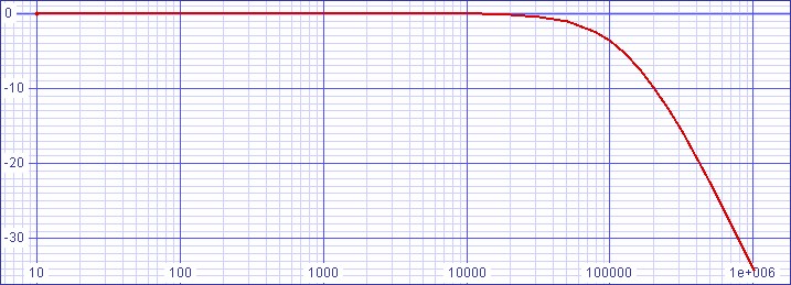
SPICE model
| Figure 2: Bode plot shows cutoff
frequency slightly lower than 100kHz goal |
 |
Distortion results are primarily second and third harmonic
Fourier analysis for vout:
No. Harmonics: 16, THD: 0.0420128 %, Gridsize: 1024, Interpolation Degree: 3
| Harmonic | Frequency | Magnitude | |
Norm.Mag | |
Percent | Decibels | |
|
|
|
|
|
|
|
|||
| 1 | 1000 | 2.69196 | 1 | 100 | 0 | |||
| 2 | 2000 | 0.00111459 | 0.000414043 | 0.0414043 | -67.65909107 | |||
| 3 | 3000 | 0.000191641 | 7.11902E-05 | 0.00711902 | -82.95159574 | |||
| 4 | 4000 | 4.70198E-06 | 1.74667E-06 | 0.000174667 | -115.1557828 | |||
| 5 | 5000 | 2.86806E-06 | 1.06542E-06 | 0.000106542 | -119.4495831 | |||
| 6 | 6000 | 9.57495E-07 | 3.55687E-07 | 3.55687E-05 | -128.9786402 | |||
| 7 | 7000 | 2.37009E-06 | 8.8043E-07 | 0.000088043 | -121.1061034 | |||
| 8 | 8000 | 1.10266E-06 | 4.09612E-07 | 4.09612E-05 | -127.7525466 | |||
| 9 | 9000 | 2.13659E-06 | 7.93694E-07 | 7.93694E-05 | -122.0069381 | |||
| 10 | 10000 | 1.07911E-06 | 4.00865E-07 | 4.00865E-05 | -127.9400372 | |||
| 11 | 11000 | 1.93559E-06 | 7.19026E-07 | 7.19026E-05 | -122.8651081 | |||
| 12 | 12000 | 4.9167E-07 | 1.82644E-07 | 1.82644E-05 | -134.7678918 | |||
| 13 | 13000 | 1.9412E-06 | 7.21108E-07 | 7.21108E-05 | -122.8399937 | |||
| 14 | 14000 | 2.00793E-07 | 7.459E-08 | 0.000007459 | -142.5463879 | |||
| 15 | 15000 | 1.45375E-06 | 5.40032E-07 | 5.40032E-05 | -125.3516101 |
Out of curiosity, without extra current bias to Q1 from R2, distortion is 0.199071%.
Signal to noise ratio:
119.6568dB relative to 1VRMS.
Relative to 2.6952VPEAK/1.90579VRMS at full-scale level add 5.60152dB for
125.258dB relative to 0dBFS.
Attempt at an Improvement
In my second try, setting R5 to a very high value to allow R3 to take a smallest possible value promises to lower distortion by allowing a design with higher bias through Q1.Design
The two synchronous pole frequencies will be 155.377kHz as they were calculated in equations 1 and 2 above.Choose VEE = 15V.
Choose VCC = –30V to give room for desired bias.
Calculate R3 and R5 to convert 3.9mA input signal to 2VRMS output signal.
| (14) |
R3
|| R5
= |
1.41421 ×
2V
3.9mA |
= 725.238Ω |
Choose R5 = 100kΩ.
Subtracting R5 from the parallel pair R3 || R5 leaves R3.
| (15) |
R3
= |
100kΩ
×
725.238Ω
100kΩ – 725.238Ω |
= 730.536Ω |
R3 = 732Ω
Calculate R2 for 5V headroom below ground:
| (16) |
IQ1
= |
30V – 5V
732Ω |
= 34.153mA |
| (17) |
IR2 = 34.153mA – 6.2mA – 3.9mA = 24.053mA |
| (18) |
R2
= |
15V
24.053mA |
= 623.623Ω |
R2 = 620Ω
Calculate C2 for second synchronous lowpass pole:
| (19) |
C2 = |
1
2πfpoleRPOLE |
= |
1
2π × 155.377kHz × (732Ω || 100kΩ) |
= 1.40958nF |
C2 = 1.3nF
To prepare to calculate for first lowpass pole, calculate an R1 value to add with the AC emitter impedance to total about 10Ω.
First calculate minimum emitter current.
| (20) |
IQ1-MIN
= |
15
620Ω |
+ 6.2mA –
3.9mA = 26.4935mA |
Then calculate maximum emitter impedance:
| (21) |
ZQ1E-MIN = |
25mA
26.4935mA |
= 943.626mΩ |
Then calculate R1.
| (22) |
R1 = 10Ω – 943.626mΩ = 9.05637Ω |
R1 = 9.1Ω
Now C1 can be calculated.
| (23) |
C1 = |
1
2πfpoleRPOLE |
= |
1
2π × 155.377kHz × (943.626mΩ + 9.1Ω) |
= 101.987nF |
C1 = 100nF
Calculate 1W R4 to dissipate ½W:
| (24) |
R4 = |
V2
P |
= |
(30V – 0.7V)2
0.5 |
= 1.71698kΩ |
R4 = 1.8kΩ
Initially I arbitrarily choose C3 = 47µF
Calculate C4 for a time constant of 1s.
| (25) |
C4 = |
T
RPOLE |
= |
1s
732Ω + 100kΩ |
= 9.92733µF |
C4 = 10µF
After some thought, I realized that loading would affect the calculation of C4 here. In the first circuit, a 10kΩ or 47kΩ load would appear insignificant in parallel with 1.43kΩ. For that reason, I originally disregarded loading there. However, here 47kΩ lowers the R5 || RL combination by more than a factor of 3. Even still, raising a calculated pole from 0.1592Hz to 0.4978Hz still may not merit an alteration to the calculated value if only a 47kΩ load is expected. However for completeness, recalculating with a 47kΩ load will give a new value for C4: 30.5766µF.
Round to nearest 10% value:
C4 = 30µF
| Parts
List |
|||
| Q1 | 2N3906 PNP |
R5 |
100kΩ 5% ¼W or ½W |
| D1 | 1N914 or 1N4148 |
C1 | 100nF 5% plastic |
| R1 |
9.1Ω 5% ¼W | C2 | 1.3nF 5% plastic |
| R2 |
620Ω % ½W | C3 | 47µF 10% aluminum electrolytic |
| R3 | 732Ω 1% 2W |
C4 | 30µF 10% plastic |
| R4 | 1.8kΩ 5% 1W | ||
Prefer to upgrade Q1 to a small-signal PNP in T0-5 package (metal can).
C1 and C2 are preferred in this order: polystyrene, teflon, polypropylene, …
C4 is preferred in this order: polypropylene, polycarbonate, polyester (Mylar), …
SPICE Analysis
SPICE model
of
improved
circuit.| Figure 3: Bode plot still shows cutoff
frequency slightly lower than 100kHz goal |
 |
Distortion results are primarily second and third harmonic
Fourier analysis for vout:
No. Harmonics: 16, THD: 0.108487 %, Gridsize: 1024, Interpolation Degree: 3
| Harmonic | Frequency | Magnitude | |
Norm.Mag | |
Percent | |
Decibels |
|
|
|
|
|
|
|
|||
| 1 | 1000 | 2.71265 | 1 | 100 | 0 | |||
| 2 | 2000 | 0.00293561 | 0.00108219 | 0.108219 | -59.31392967 | |||
| 3 | 3000 | 0.000206089 | 7.59733E-05 | 0.00759733 | -82.38678018 | |||
| 4 | 4000 | 0.000010125 | 3.7325E-06 | 0.00037325 | -108.5600037 | |||
| 5 | 5000 | 4.86714E-06 | 1.79424E-06 | 0.000179424 | -114.9223893 | |||
| 6 | 6000 | 6.40395E-08 | 2.36078E-08 | 2.36078E-06 | -152.5388897 | |||
| 7 | 7000 | 5.0589E-06 | 1.86493E-06 | 0.000186493 | -114.5867493 | |||
| 8 | 8000 | 6.24975E-08 | 2.30393E-08 | 2.30393E-06 | -152.7506144 | |||
| 9 | 9000 | 4.0545E-06 | 1.49467E-06 | 0.000149467 | -116.5090936 | |||
| 10 | 10000 | 4.22788E-07 | 1.55858E-07 | 1.55858E-05 | -136.145418 | |||
| 11 | 11000 | 2.47042E-06 | 9.10705E-07 | 9.10705E-05 | -120.8124456 | |||
| 12 | 12000 | 3.31809E-07 | 1.22319E-07 | 1.22319E-05 | -138.2501216 | |||
| 13 | 13000 | 1.05783E-06 | 3.89963E-07 | 3.89963E-05 | -128.1795319 | |||
| 14 | 14000 | 6.45024E-07 | 2.37784E-07 | 2.37784E-05 | -132.4763474 | |||
| 15 | 15000 | 4.6302E-07 | 1.70689E-07 | 1.70689E-05 | -135.3558893 |
Signal to noise ratio:
117.8938dB relative to 1VRMS.
Relative to 2.72627VPEAK/1.92776VRMS at full-scale level add 5.70108dB for
123.595dB relative to 0dBFS.
Result of Change
Paradoxically, the improvement has increased the distortion. I believe this result is due to distortion having some inversely proportional relationship to the value of R2 as well at to the current bias change. Because primarily the second harmonic was raised leaving the third harmonic the same this change becomes a more euphonic preference. Perhaps even more important the change allows the use of a lower distortion capacitor at C4. The second circuit is not recommended to drive loads lower than 47kΩ.Design an NPN circuit
| Figure 4: Schematic of
single-ended analog circuit |
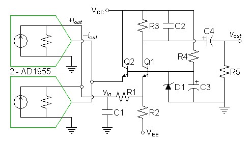 |
| Note: Only left channel shown. Duplicate for the right channel. |
This NPN circuit is only flipped in polarity from the PNP circuit
first introduced apart from two details: That this circuit is
biased with a zener rather than an normal diode because the particular
DAC requires its current output to sink into a non-zero voltage and the
decision to use two DACs.
Evaluate Datasheet
The datasheet for the AD1955 gives the following output specifications:| AC output |
|
8.64mA peak-to-peak differential 2.16mA peak single ended |
| DC offset |
–3.24mA (specified as current
sink) |
|
| Output impedance |
Unspecified |
|
| Analog sink voltage |
2.80V ideal, down to low of 2.39V |
Analyzing polarity of reference analog circuit suggests no polarity reversal for connection. Because the output current specifications are expected to design to a high output impedance, use two parallel devices.
As a parallel pair their specifications are now:
| AC output |
|
17.28mA peak-to-peak differential 4.32mA peak single ended |
| DC offset |
-6.48mA (specified as current
sink) |
|
| Output impedance |
Unspecified |
|
| Analog sink voltage |
2.80V ideal, down to low of 2.39V |
Design
Begin by calculating two synchronous pole frequencies which together will roll off at 100kHz:
|
|
|
| (27) |
fstage
= |
fsystem
α |
= |
100kHz
0.643594 |
= 155.377kHz |
Choose VEE = –15V
Choose VCC = 30V to give room for desired bias.
Assume rated output current is dropped between the optimal output sink voltage and ground. Then calculate DAC output impedance:
| (28) |
RDAC
= |
VSINK
– GND
IDAC-MAX |
= |
2.8V - 0V
6.48mA + 4.32mA |
= 259.259Ω |
Calculate D1 zener voltage
| (29) |
Vzener-D1
= 2.8V + 0.7V = 3.5V |
Vzener-D1 = 3.3V
Operating sink voltage will now be:
.VSINK = 2.6V
Calculate R3 and R5 to convert 3.9mA input signal to 2VRMS output signal
| (30) |
R3
= |
2 ×
1.41421 ×
2V
4.32mA |
= 1.30946kΩ |
R3 and R5 = 1.33kΩ
Here, I decided to round up to compensate for the slight loss of signal current to the current divider created by RDAC and R1.
Calculate R2 for 5V headroom below ground:
| (31) |
IQ1
= |
30V - 5V -
3.3V
1.33kΩ |
= 16.3158mA |
| (32) |
IR2 = 16.3158mA - 6.48mA - 2.16mA = 7.67579mA |
| (33) |
R2
= |
15V + 2.6V
7.67579mA |
= 2.29292kΩ |
R2 = 2.4kΩ
Calculate C2 for second synchronous lowpass pole:
| (34) |
C2 = |
1
2πfpoleRPOLE |
= |
1
2π × 155.377kHz × (1.33kΩ/2) |
= 1.54032nF |
C2 = 1.5nF
To prepare to calculate for first lowpass pole, calculate an R1 value to add with the AC emitter impedance to total about 10Ω.
First calculate minimum emitter current.
| (35) |
IQ1-MIN
= |
15V + 2.6V
2.4kΩ |
+ 6.48mA -
4.32mA = 9.49333mA |
Then calculate maximum emitter impedance:
| (36) |
ZQ1E-MIN = |
25mV
9.49333mA |
= 2.63343Ω |
Then calculate R1.
| (37) |
R1 = 10Ω – 2.63343Ω = 7.36657Ω |
R1 = 7.5Ω
Now C1 can be calculated.
| (38) |
C1 = |
1
2πfpoleRPOLE |
= |
1
2π × 155.377kHz × (2.63343Ω + 7.5Ω) |
= 101.083nF |
C1 = 100nF
Calculate 1W R4 to dissipate ½W:
| (39) |
R4 = |
V2
P |
= |
(30V – 3.3V)2
0.5 |
= 1.42578kΩ |
R4 = 1.5kΩ
Arbitrarily chose C3 = 47µF.
Calculate C4 for a time constant of 1s.
| (40) |
C4 = |
T
RPOLE |
= |
1s
1.33kΩ + 1.33kΩ |
= 375.94µF |
C4 = 390µF
| Parts
List |
|||
| Q1,Q1 | 2N3904 PNP |
R5 |
1.33kΩ 1% ½W or 1W |
| D1 | 3.3V zener |
C1 | 100nF 5% plastic |
| R1 |
7.5Ω 5% ¼W | C2 | 1.5nF 5% plastic |
| R2 |
2.4kΩ % ½W | C3 | 47µF 10% aluminum
electrolytic |
| R3 | 1.33kΩ 1% 1W |
C4 | 390µF 10% aluminum electrolytic |
| R4 | 1.5kΩ 5% 1W | ||
Prefer to upgrade Q1 to a small-signal NPN in T0-5 package (metal can).
C1 and C2 are preferred in this order: polystyrene, teflon, polypropylene, …
SPICE Analysis
SPICE model| Figure 5: Bode plot still shows cutoff
frequency slightly lower than 100kHz goal |
 |
Fourier analysis for vout:
No. Harmonics: 16, THD: 0.0415427 %, Gridsize: 1024, Interpolation Degree: 3
| Harmonic | Frequency | Magnitude | |
Norm. Mag | |
Percent | Decibels | |
|
|
|
|
|
|
|
|||
| 1 | 1000 | 2.847 | 1 | 100 | 0 | |||
| 2 | 2000 | 0.00117564 | 0.000412941 | 0.0412941 | -67.6822 | |||
| 3 | 3000 | 0.000128299 | 4.50648E-05 | 0.00450648 | -86.9233 | |||
| 4 | 4000 | 1.39636E-05 | 4.90466E-06 | 0.000490466 | -106.188 | |||
| 5 | 5000 | 4.21864E-06 | 1.48179E-06 | 0.000148179 | -116.584 | |||
| 6 | 6000 | 5.05001E-07 | 1.7738E-07 | 0.000017738 | -135.022 | |||
| 7 | 7000 | 2.64547E-06 | 9.29215E-07 | 9.29215E-05 | -120.638 | |||
| 8 | 8000 | 1.00591E-06 | 3.53324E-07 | 3.53324E-05 | -129.037 | |||
| 9 | 9000 | 1.88327E-06 | 6.61494E-07 | 6.61494E-05 | -123.589 | |||
| 10 | 10000 | 7.95153E-07 | 2.79295E-07 | 2.79295E-05 | -131.079 | |||
| 11 | 11000 | 1.15167E-06 | 4.0452E-07 | 0.000040452 | -127.861 | |||
| 12 | 12000 | 1.5341E-07 | 5.38848E-08 | 5.38848E-06 | -145.371 | |||
| 13 | 13000 | 1.31741E-06 | 4.62736E-07 | 4.62736E-05 | -126.693 | |||
| 14 | 14000 | 2.86087E-07 | 1.00487E-07 | 1.00487E-05 | -139.958 | |||
| 15 | 15000 | 1.11035E-06 | 3.90009E-07 | 3.90009E-05 | -128.179 |
Signal to noise ratio:
122.0053dB relative to 1VRMS.
Relative to 2.847VPEAK/2.01313VRMS at full-scale level add 6.07745dB for
128.083dB relative to 0dBFS.
|
|
Document History
December 1, 2012 Created.
December 1, 2012 Added equation numbers to design
and some extra text and rescinded 750µF
calculation for C3.
December 1, 2012 Added a second design sequence aimed to improve
distortion.
December 2, 2012 Added text recalculating a new C4 value for the
second circuit under load.
December 4, 2012 Corrected 25mA in equation 9 to 25mV.
December 7, 2012 Correcting SPICE model error changed distortion
results somewhat. Reworded statement about useful DACs to
indicate that the AD1955 will require an NPN design. Added
paragraph on the interpretation of the datasheet.
January 1, 2013 Added an NPN design and analysis based on the
AD1955.
January 2, 2013 Changed schematics to show how unused DAC outputs
should be terminated.